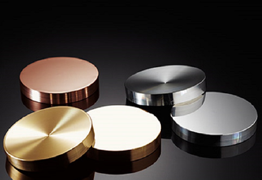
What are the Primary Performances Requirements of Target Materials?
Purity
Purity is one of the main performance indexes of target materials because the purity of target materials has a great influence on the performance of thin films. However, the purity requirements of target materials are not the same in practical application. For example, with the rapid development of the microelectronics industry, the size of the silicon wafer has increased from 6 “and 8” to 12 “, and the wiring width decreased from 0.5um to 0.25um, 0.18um, and even 0.13um. Previously, the purity of target material was 99.995%, which could meet the technical requirements of 0.35umic, while the purity of target material was 99.999% or even 99.9999% for the preparation of 0.18um line.
Impurity content
The impurities in the solid of the target material and the oxygen and water vapor in the stoma are the main pollution sources of the deposition film. The requirements for different impurities in different target materials are also different. For example, pure aluminum and aluminum alloy target materials used in the semiconductor industry have special requirements on the content of alkali metal and radioactive elements.
Density
In order to reduce the porosity and improve the properties of the sputtering film, high density of target material is usually required. The density of the target material affects not only the sputtering rate but also the electrical and optical properties of the film, the higher the density of the target material, the better the performance of the film. In addition, increasing the density and strength of the target material enables the target material to better withstand the thermal stress during sputtering, and density is one of the key performance indicators of the target material.
Grain size and grain size distribution
The target material is usually polycrystalline and the grain size can range from micron to millimeter. For the same target material, the sputtering rate of the target with small grain size is faster than that of the target with large grain size; the thickness distribution of target sputtering films with small grain size difference is more uniform.
Stanford Advanced Materials (SAM) Corporation is a global sputtering target manufacturer established in 1994. For more information, please visit https://www.sputtertargets.net/.


