Applications of Copper Plating Technology on TSV and LCD Panels
Copper plating is one of the most widely used pre-plated layers in the electroplating industry, including solder joints, lead-tin alloys, and zinc die-casting parts. Two important applications for copper plating are on TSV and LCD panels.
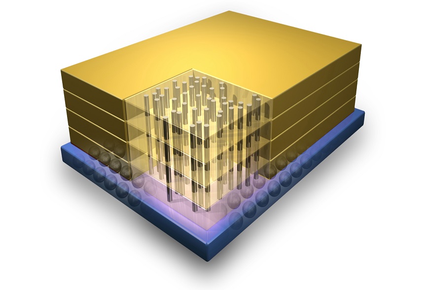
Through Silicon Via (TSV)
One developing application for copper plating technology is through-silicon via (TSV) 3D integration. The goal of 3D integration of chips is to create semiconductor devices that run faster, are cheaper, and are smaller. At present, 3D integration is mostly made by miniaturizing circuits and components, using wire bonding and flip chip integration technology. Wire bonding can result in loss of inductance, which can impair the performance of the chip. One way to improve wire bonding is to use through-silicon via technology. Essentially, two or more vertically integrated chips are connected together by a vertical interconnect operation that functions like an IC component. In copper electroplating, the barrier film is a very important part. It should not be too thick (to make copper lose high conductivity), and not too thin (it must be able to completely separate copper). Tantalum target is an excellent choice for barrier films in copper plating, and is therefore widely used in copper plating.
LCD panel
Copper plating technology is also widely used in thin film LCD panel displays. These interconnections are used to generate pixels and form colors through color filters. Copper interconnects have low conductivity, which are approximately 60% lower than aluminum interconnects, and are capable of transmitting media signals through large LCD screens without noise, resulting in sharp images with little distortion or display vibration. Large-area targets used in a TFT-LCD are generally planar targets, but since large-area rotatory targets have an advantage of high material utilization efficiency, they have also been applied to a liquid crystal panel. However, although we mentioned in a previous article Application of Tantalum Target in Thermal Inkjet Print Head and Copper Plating that tantalum targets are widely used in copper plating technology, so far in the TFT-LCD manufacturing process, copper plating technology has chosen titanium target instead of tantalum target as a barrier layer.
Stanford Advanced Materials (SAM) Corporation is a global supplier of various sputtering targets and evaporation materials such as metals, alloys, oxides and ceramic materials, which are widely used in multiple industries. We regularly update knowledge and interesting stories of sputtering targets on our website, and if you like this article, please share it to your friends.


