Application of Tantalum Target in Thermal Inkjet Print Head and Copper Plating
Since tantalum has the ability to form oxides thin film, which has a protective effect, the tantalum target is widely used as a base material for electrolytic capacitor manufacturing. This article introduces the application of tantalum sputtering targets in the field of microelectronics.
 Sputtering Target")
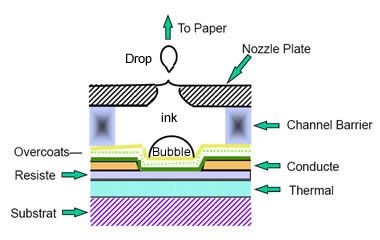
Tantalum for Thermal Inkjet Print Head Application
Thermal inkjet print heads can be used in the fabrication of thin film integrated circuits, which facilitates the use of tantalum target. In the manufacturing process of integrated circuits, a thin film resistor is used to rapidly heat the film layer of the ink at an energy density close to 1.28E9 watt/m2, so that some very small portions of the ink are evaporated to form extension bubbles, which are actually small droplets of ink that are ejected. Since high-temperature inks can cause cavitation in some ink-jet printing apparatuses, the use of tantalum anti-cavitation films can protect the ink facilities.
Tantalum Target for Copper Plating Application
Tantalum films have obvious advantages in the manufacturing process of integrated circuits, and a major advance in the use of tantalum sputtering target is the application of copper plating. Photoresist masks and plasma etching techniques cannot be used to form copper because copper does not form the desired volatile components under low-temperature plasma etching conditions. Since copper has high electrical conductivity, the barrier film must be able to completely isolate copper. However, if the barrier film is too thick, it will lose the high conductivity advantage of the copper interconnect. Therefore, it is important that the deposition of the barrier film in the copper plating scheme has good step coverage and that the protrusion is to be reduced at the channel/trench void. In the replacement of 0.10 um copper integrated circuits, tantalum and tantalum nitric oxide PVD barrier films have shown some unique advantages, such as good copper diffusivity and good adhesion to electrolytes and copper.
We’ve talked about the application of tantalum target in thermal inkjet print head and copper plating. From the above contents, we can learn that tantalum is a potential material in microelectronic industry. Believe it or not, these are just part of the applications of the tantalum sputter target. If you are interested in this topic, please pay attention to our website https://www.sputtertargets.net/ for subsequent updates. We regularly update knowledge and interesting stories about sputtering targets, and if you like this article, please share it to your friends.


