Sputtering Target: An Important Component of Semiconductor Materials
Semiconductor materials can be divided into wafer materials and packaging materials. Compared with wafer manufacturing materials, packaging materials have relatively low technical barriers, so we mainly talk about wafer manufacturing materials. The production of wafer mainly involves 7 kinds of semiconductor materials and chemicals, each of which accounts for the following proportion in the semiconductor material market: silicon wafer, 33%; specialty gases, 17%; mask plate, 15%; ultra-clean high purity reagent, 13%; polishing fluid and polishing pad, 7%; photoresist material, 7%; sputtering target, 3%.
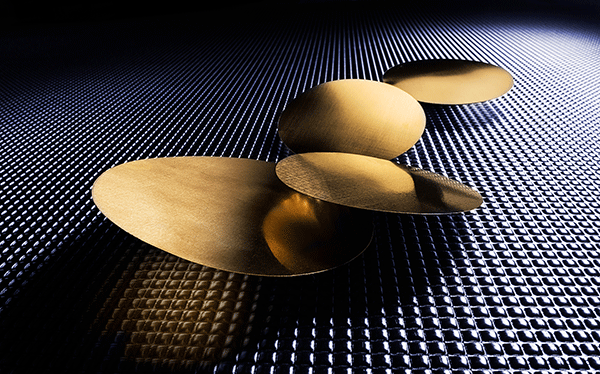
Today we are mainly talking about sputtering target materials with a proportion of about 3% in the semiconductor material market. The sputtering target is the target material of high-speed charged particle bombardment. Different film systems (such as super-hard, wear-resistant, anti-corrosion alloy film, etc.) can be obtained by changing different target materials (such as aluminum, copper, stainless steel, titanium, nickel target, etc.).
According to different chemical compositions, the sputtering target materials can be divided into metal target materials (pure metal aluminum, titanium, copper, tantalum, etc.), alloy target material (nickel-chrome alloy, nickel-cobalt alloy, etc.) and ceramic compound target materials (oxides, silicides, carbides, sulfide, etc.); according to different application fields, it can be divided into semiconductor chip target material, planar display target material, solar cell target material, information storage target material, tool modified target material, electronic device target material, and other target materials.
The inner part of the semiconductor is composed of tens of thousands of meters of metal wiring, and the sputtering target material is the key consumption material for making these wiring. Apple’s A10 processor, for example, has a chip the size of a nail covered with tens of thousands of meters of metal wires that have to be splattered onto a high-purity metal target. The sputtering target material is the core of semiconductor wafer manufacturing, and the chip has very high requirements for sputtering target material, which requires high purity of target material, generally over 99.999%.
Application and market structure
How do you know which metal is used in a few inches of the wafer and which is used in advanced manufacturing processes? In semiconductor wafer manufacturing, the manufacturing process of 200mm (8-inch) and below wafers is usually mainly made of aluminum, and the target materials used are mainly made of aluminum and titanium. However, the manufacture of 300mm (12-inch) wafer mostly uses advanced copper interconnection technology and mainly uses copper and tantalum target materials.
Overall, as the use of chips more and more extensive and the number of chip market demand increased, the demand for aluminum, titanium, tantalum and copper, the four mainstream thin film metals in the industry, will also increase. There is currently no alternative to the four thin film materials, either technically or economically, so they are not at risk of being replaced.
The sputtering coating technology originated from abroad and the required sputtering target products have high-performance requirements, so the research and production of the sputtering target in the world are mainly concentrated in a few companies in the United States and Japan for a long time, and the industrial concentration is quite high. The application fields of sputtering target mainly focus on semiconductor industry, flat panel display industry (including touch screen industry) and solar cell industry.
Stanford Advanced Materials (SAM) Corporation is a global sputtering target manufacturer established in 1994. For more information, please visit https://www.sputtertargets.net/.


