(949) 407-8904 Mon - Fri 08:00 - 17:00 1940 East Deere Avenue, Suite 100, Santa Ana, CA 92705, USA

ST11219 Zinc (Zn) Planar Sputtering Target

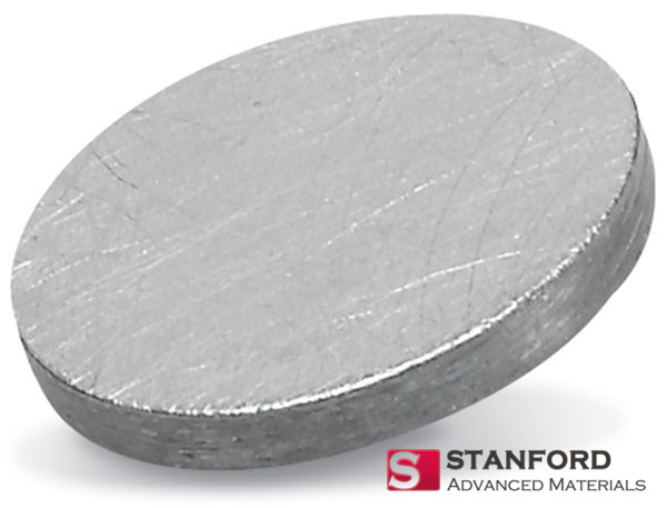
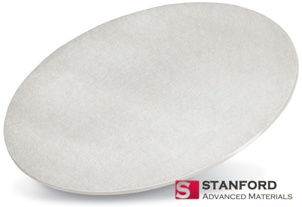
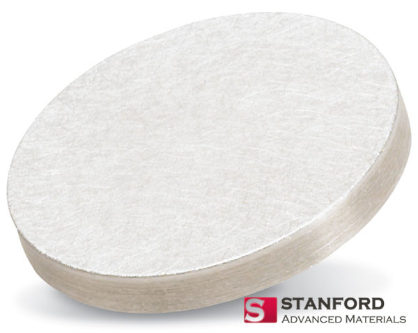
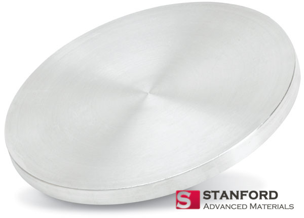
Our Zinc (Zn) Planar Sputtering Targets are manufactured from high-purity elemental zinc, serving as a fundamental source material for depositing conductive, transparent, and protective thin films. Zinc’s relatively low melting point and high vapor pressure make it an efficient sputtering source for applications ranging from transparent electrodes in solar cells to sacrificial anti-corrosion coatings in harsh environments.

Product Code ST11219 (Standard Reference)
Material Zinc (Zn)
Typical Purity ≥ 99.99% (4N)
Form & Shape Planar Sputtering Target (Rectangular/Disc)
Key Properties Low Melting Point (~420°C) | High Vapor Pressure | Excellent Sacrificial Corrosion Protection
Key Advantage Provides an efficient, high-purity source for depositing zinc films and, through reactive sputtering, high-quality zinc oxide (ZnO)—a versatile semiconductor with wide applications in optoelectronics and sensing.

Key Advantage: Enables deposition of pure zinc for corrosion protection or as a dopant source, and serves as the primary target for reactive sputtering of ZnO—a key material for transparent conductive oxides (TCOs) and piezoelectric devices.

Customization: Purity (99.99% to 99.9999%), dimensions (thickness, width, length), bonding, and surface finish are fully customizable to match specific deposition systems and process requirements.

Primary Applications: Precursor for aluminum-doped zinc oxide (AZO) TCOs in solar cells and displays; sacrificial anti-corrosion coatings (galvanic protection); seed layers for ZnO nanowire growth; dopant source in compound semiconductors; transparent electrodes in touch panels.


Description

Complete Technical Specifications & Capabilities

Comprehensive specifications for sputtering zinc films and reactive deposition of zinc oxide.

Parameter Specification / Details
Material Zinc (Zn)
Typical Purity ≥ 99.99% (4N Standard), 5N and 6N available
Crystal Structure Hexagonal Close-Packed (HCP)
Density 7.14 g/cm³
Melting Point 419.5 °C (787.1 °F)
Vapor Pressure Relatively high at typical sputtering temperatures
Standard Shape Planar – Rectangular, Circular (Disc)
Dimensions Fully Customizable (Thickness, Width, Length, Diameter)
Surface Finish Machined and cleaned to minimize oxides; can be supplied with protective coating
Bonding Option Available bonded to Cu or Al backing plates using low-temperature solders (e.g., In) or elastomer bonding due to Zn’s low melting point
Manufacturing Method High-purity casting, rolling, and machining under controlled atmosphere
Special Handling Note Zinc is relatively soft and can oxidize; targets are typically packaged under inert gas or with desiccants
Quality Documentation Certificate of Analysis with GDMS/ICP purity verification

Technical & Application Deep Dive

1. The Gateway to Zinc Oxide (ZnO): A Multifunctional Semiconductor

The primary use of high-purity zinc targets is for reactive sputtering of ZnO, a material with exceptional versatility:

  • Transparent Conductive Oxides (TCOs): When doped with aluminum (Al), ZnO becomes aluminum-doped zinc oxide (AZO)—a highly transparent, conductive, and cost-effective alternative to indium tin oxide (ITO) for solar cells, flat-panel displays, and touch screens.
  • Piezoelectric Devices: ZnO’s strong piezoelectric properties make it ideal for surface acoustic wave (SAW) filters, sensors, and micro-electromechanical systems (MEMS).
  • UV Optoelectronics: With a direct bandgap of ~3.37 eV, ZnO is used in UV LEDs, detectors, and lasers.
  • Buffer Layers in Thin-Film Photovoltaics: Used in CIGS and perovskite solar cells to improve interface properties and device efficiency.

2. Pure Zinc Films: Functional Coatings and Alloying

Metallic zinc films also serve important purposes:

  • Sacrificial Anti-Corrosion Coatings: Zinc acts as a sacrificial anode, providing galvanic protection to steel and other metals. Sputtered zinc films offer a uniform, controlled alternative to hot-dip galvanizing for precision components.
  • Seed Layers for Nanostructures: Thin zinc films serve as catalysts or seed layers for the subsequent growth of ZnO nanowires or nanostructures via thermal oxidation or other methods.
  • Alloying Component: Used in co-sputtering to create zinc-containing alloys (e.g., brass, Zn-Sn, Zn-Mg) for specialized coating applications.
  • Dopant Source: In III-V semiconductor manufacturing, zinc is a common p-type dopant; sputtering from a Zn target can be used for doping during epitaxial growth.

3. Sputtering Process Considerations for Zinc

Sputtering zinc requires attention to its specific material properties:

  • Low Melting Point: Requires careful control of sputtering power and target cooling to prevent localized melting or thermal runaway.
  • High Deposition Rate: Zinc’s high sputtering yield allows for high deposition rates, improving coating throughput.
  • Reactive Sputtering for ZnO: Adding oxygen to the sputtering gas allows for the deposition of stoichiometric or oxygen-deficient ZnO films. Process control is key to obtaining the desired optical and electrical properties.
  • Oxidation Sensitivity: Pure zinc targets must be handled and stored to minimize surface oxidation, which can affect initial sputtering stability.

Quality Assurance & Manufacturing

Stanford Advanced Materials ensures the highest quality for zinc targets:

  • High-Purity Production: Raw materials are refined to 4N (99.99%) purity or higher, with trace element analysis via Glow Discharge Mass Spectrometry (GDMS).
  • Oxidation Control: Manufacturing and final machining are performed in controlled atmospheres or with coolant systems that minimize oxide formation on the target surface.
  • Dimensional Accuracy: Precision machining ensures flatness and dimensional tolerances required for proper thermal contact and even erosion in the sputtering system.
  • Protective Packaging: Targets are sealed with desiccants or under inert gas to preserve surface quality during shipping and storage.

Why Choose SAM for Your Zinc Targets?

  • Optoelectronics & PV Focus: We specialize in high-purity materials for transparent conductive oxides and photovoltaic applications, understanding the critical link between target purity and film performance.
  • Superior Purity Control: Our 4N standard purity ensures low contamination levels for high-performance ZnO films, with options for even higher purity for advanced research.
  • Expertise in Reactive Sputtering Materials: We provide technical guidance on target specifications optimized for stable, reproducible reactive sputtering processes to produce high-quality ZnO.
  • Custom Solutions: We tailor target dimensions, bonding, and packaging to your specific system and process flow, from lab-scale R&D to production coating.

Next Steps: Get a Custom Quote

To receive a formal quotation or technical consultation, please provide:

  1. Required purity (e.g., 99.99%, 99.999%).
  2. Target dimensions (Thickness x Width x Length or Diameter x Thickness) and shape.
  3. Primary application (e.g., AZO for TCO, ZnO piezoelectric films, pure Zn corrosion coating).
  4. If for reactive sputtering, any specific film property goals (e.g., resistivity, transparency).
Request a Quote