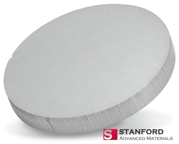
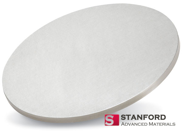
Our Indium Planar Sputtering Targets are manufactured from the highest purity indium metal, making them ideal for depositing ultra-clean, low-resistance films essential for ohmic contacts on sensitive semiconductors, as a component in ITO (Indium Tin Oxide) deposition, and for specialized low-temperature bonding layers where purity is paramount.
| Material | Indium (In) |
| Purity | ≥ 99.99% (4N) Standard |
| Key Property | Low Melting Point (156.6°C), High Purity |
| Form | Planar Sputtering Target |
Key Advantage: Exceptionally low levels of metallic impurities (e.g., Pb, Sn, Cd, Tl) prevent doping or poisoning of sensitive semiconductor interfaces and ensure optimal performance in optoelectronic devices.
Customization: Purity (up to 99.999%), dimensions (thickness, length, width), and bonding fully customizable.
Typical Applications: Ohmic contacts for compound semiconductors (GaAs, InP, GaN), component target for ITO co-sputtering, superconducting junction layers, and low-temperature solder/bonding films.
For detailed evaluation and procurement (Standard Reference: ST11190).
| Parameter | Specification / Typical Value |
|---|---|
| Material | Indium (In) |
| Purity (Standard) | ≥ 99.99% (4N) |
| Available Purity | 99.99%, 99.995%, 99.999% |
| Density | ≥ 7.28 g/cm³ (Theoretical: 7.31 g/cm³) |
| Melting Point | 156.6 °C |
| Electrical Resistivity | ~8.4 µΩ·cm (20°C) |
| Thermal Conductivity | 82 W/(m·K) |
| Standard Shape | Rectangular |
| Dimensions | Fully Customizable (Thickness ≥ 3mm recommended) |
| Sputtering Method | DC Magnetron (Low Power Recommended) |
| Bonding Options | Low-temperature bonding to Cu or Mo backing plates |
| Certification | Certificate of Analysis (CoA) with GDMS/ICP-MS data provided |
1. Critical Purity for Semiconductor Interfaces
In advanced III-V semiconductors (e.g., GaAs, InP) and wide bandgap devices (e.g., GaN), indium is often used as a low-resistance ohmic contact material. Trace metallic impurities at the semiconductor-metal interface can create deep-level traps, increase contact resistance, and degrade device reliability and high-frequency performance. Our ≥99.99% purity, with specific impurity control, is engineered to mitigate these risks.
2. A Key Component for Transparent Conductive Oxides
Indium is the essential, high-cost component in Indium Tin Oxide (ITO), the dominant transparent conductive film. While ITO is often sputtered from a ceramic ITO target, an alternative process is reactive co-sputtering from separate high-purity Indium and Tin metal targets in an oxygen atmosphere. Our indium targets are designed for this precise co-sputtering process, allowing fine-tuning of the In:Sn ratio for optimal film properties.
3. Handling and Process Considerations
Indium is a very soft metal with a low melting point. This requires special handling and sputtering precautions:
4. Niche Applications Leveraging Unique Properties
For indium, purity analysis is critical. We utilize Glow Discharge Mass Spectrometry (GDMS) or Inductively Coupled Plasma Mass Spectrometry (ICP-MS) to provide parts-per-billion (ppb) level quantification of key impurities that are detrimental to electronic applications. This high-sensitivity certification is what differentiates our targets for research and high-end manufacturing.
Get a Formal Quote or CoA Sample
To specify the indium target for your sensitive application, please provide: