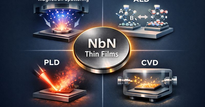
(949) 407-8904 Mon - Fri 08:00 - 17:00 1940 East Deere Avenue, Suite 100, Santa Ana, CA 92705, USA

Company Dynamic

optimize-target-tco

Semiconductor Target TCO Analysis: Boosting Utilization by 30% via Design & Bonding

Abstract: In semiconductor manufacturing, the cost of a PVD sputtering target extends far beyond its purchase price. For 300mm targets, low utilization rates and unscheduled downtime due to bonding failures represent massive, hidden costs. This article provides a Total Cost of Ownership framework, demonstrating how strategic target design (rotary vs. planar, asymmetric erosion profiles) and advanced...
Continue Reading
3D-NAND-COVER

PVD Targets for DRAM & 3D NAND Manufacturing: From Capacitor Electrodes to Step Coverage

Abstract: The divergence in memory architecture between DRAM and 3D NAND Flash presents unique thin-film deposition challenges, directly impacting cost and performance. This article dissects the critical PVD target strategies for both technologies: the pursuit of seamless, high-aspect-ratio fill for DRAM capacitors, and the battle for conformal step coverage in 3D NAND’s towering staircases. We...
Continue Reading
3nm 2nm chips

Key PVD Target Guide for 3nm/2nm Nodes: Selecting Cobalt & Ruthenium Barrier Layers

As the semiconductor industry advances beyond the 5nm node, conventional barrier/liner materials, such as Ta/TaN, are approaching their physical limits. This article provides a technical point of view of the two most promising successors: Cobalt (Co) and Ruthenium (Ru) PVD targets. We compare their material properties, process integration challenges, and selection criteria for advanced FinFET and...
Continue Reading

What is Chemical Vapor Deposition (CVD)? The Ultimate Guide

Introduction Chemical Vapor Deposition (CVD) might sound like an obscure lab technique, but it’s the invisible engine behind modern technology. It’s what makes your smartphone processor faster, your new sunglasses more scratch-resistant, and a jet engine withstand infernal temperatures. In essence, CVD is the art of turning a gas into a perfect solid coating, and...
Continue Reading

Case Study: Ensuring Optimal Performance of IGZO Sputtering Targets through Expert Preconditioning Guidance

Client: A leading thin-film deposition research facility Challenge: Uncertainty in preconditioning and operating a non-conductive IGZO sputtering target on a specific indirect-cooled cathode system. Solution: Stanford Advanced Materials provided detailed, system-aware technical guidance, bridging material science and equipment engineering. Result: Enabled the client to establish a safe, effective, and stable deposition process, preventing target damage and ensuring consistent film...
Continue Reading
Advanced Production Techniques for Metal Alloy Sputtering Target Manufacturing

Advanced Production Techniques for Metal Alloy Sputtering Target Manufacturing

Introduction For many years, producing metal alloy sputtering targets has been a work of precision and care. The art of turning raw metal into a tool that responds well to sputtering methods requires careful thought over the metallurgical properties at every step. Today, we will take a stroll through the laboratories and mechanical shops where...
Continue Reading
1 2 3 48