Applications and Requirements of Titanium Sputtering Target in High-Tech Industries
Requirements of Titanium Sputtering Target
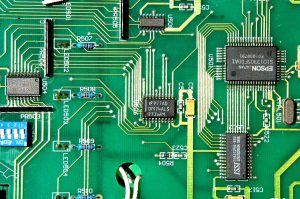
Titanium sputtering target is widely used in high-tech fields, such as electronics, information industry, home decoration, automobile glass manufacturing, etc. In these industries, titanium target is mainly used for coating the surface of components, such as integrated circuits, flat panel displays, or as a decorative coating, glass coating, etc.
Different industries have different requirements for titanium targets. Let’s take titanium circuits for an example. Usually, we use the following performance evaluation indexes to determine whether the sputtering target meets the requirements:
(1) Purity,
(2) Microstructure,
(3) Welding performance and
(4) Dimensional accuracy.
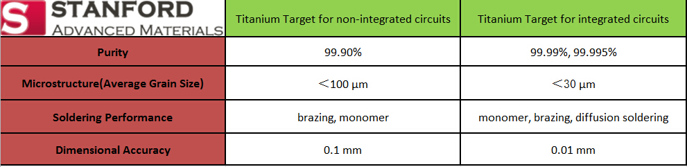
As you can see in the above table, the requirements of titanium sputtering target for non-integrated circuits and integrated circuits are different. Generally speaking, integrated circuits have high requirements on their coating materials, such as higher purity, smaller grain size, and more precise dimensional accuracy. It’s just an example, but it reveals that different industries require different for titanium targets. While you’re looking for a titanium target for your project, make sure you know the exact specifications of the product you want, which helps save your time and money.
Titanium Target Used in Integrated Circuits
From the above table, we know that the purity requirement of the integrated circuit titanium targets is mainly greater than 99.995%, which is higher than those used in non-integrated circuit. Limited by technology, the production of high-purity titanium targets is mainly in the United States and Japan. Representative companies include Honeywell and Stanford Advanced Materials in the United States, OSAKA and Toho Titanium in Japan.
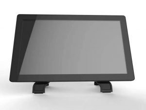
Titanium Target Used in Flat Panel Display
The flat panel display includes a liquid crystal display (LCD), a plasma display (PDP), an electroluminescent display (E-L), and a field emission display (FED). Sputter coating technologies are often used to deposit the film of the flat panel display. Al, Cu, Ti, and Mo are the main metal sputtering targets for flat panel displays. The purity of a titanium target for a flat panel display generally needs to be greater than 99.9%.
Structural Development of Titanium Target
Phase one:
Early chip foundries had large profit margins. They mainly used 100-150mm magnetron sputtering machines, whose power was small. The sputtered film was thick, and the chip size was large. At that time, titanium target for integrated circuits was mainly 100-150mm monomer and combined target.
Phase two:
In the second stage, according to Moore’s Law, the chip line width is narrowed. In order to increase the profit margin, the chip foundry has increased the sputtering power of the machine, mainly using a 150-200mm sputtering machine. This requires an increase in the size of the target while maintaining high thermal conductivity, low price and a certain strength. During this period, the titanium target was mainly composed of aluminum alloy backplate diffusion welding and copper alloy back plate brazing and welding.
Phase three:
In the third stage, as the integrated circuit develops, the chip line width is further narrowed. At this time, the chip foundry mainly uses a 200-300mm sputtering machine, and the requirements for the target are more stringent. In this period, the Ti target is mainly made of copper alloy back plate diffusion welding.
Thanks for reading this passage and hope that you now have a basic understanding of titanium target in high-tech industries. Stanford Advanced Materials (SAM) is a leading sputtering target manufacturer based in Lake Forest, California. If you feel interested in the titanium targets, you can go to our product page for more information, or directly send us an inquiry. You can also contact us via target@samaterials.com. Free samples are available.


