Chemical Formula: Pb/Se/Te
Catalog Number: ST0501
CAS Number: 12412-93-0
Purity: 99%~99.999%
Shape: Discs, Plates, Column Targets, Step Targets, Custom-made
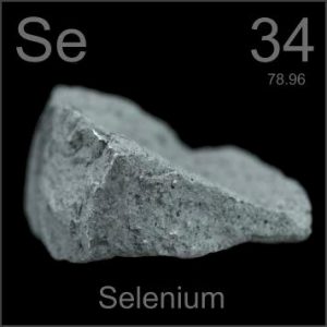
At SAM, we provide a range of Lead Selenide Telluride Sputter Targets in different forms, purities, sizes, and prices. Our expertise lies in producing high-purity physical vapor deposition materials, optimized for use in semiconductor, chemical vapor deposition, and physical vapor deposition applications in displays and optics. If you require further information or have specific inquiries, feel free to contact us.
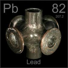
 Lead, also called plumbum, is a chemical element that originated from the Anglo-Saxon lead (plumbum in Latin). It was early used in 7000 BC and discovered by people from the Near East. “Pb” is the canonical chemical symbol of lead. Its atomic number in the periodic table of elements is 82 with location at Period 6 and Group 14, belonging to the p-block. The relative atomic mass of lead is 207.2(1) Dalton, the number in the brackets indicating the uncertainty.

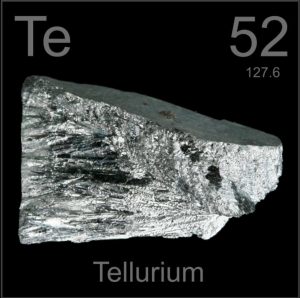
 Tellurium is a chemical element that originated from Earth, the third planet in the solar system (with the Latin word tellus). It was first mentioned in 1782 and observed by F.-J.M. von Reichenstein. The isolation was later accomplished and announced by H. Klaproth. “Te” is the canonical chemical symbol of tellurium. Its atomic number in the periodic table of elements is 52 with location at Period 5 and Group 16, belonging to the p-block. The relative atomic mass of tellurium is 127.60(3) Dalton, the number in the brackets indicating the uncertainty.
Related Products: Lead Sputtering Target, Selenium Sputtering Target, Tellurium Sputtering Target.
| Material Type | Lead Selenide Telluride |
| Symbol | Pb/Se/Te |
| Color/Appearance | Gray metallic solid in various forms |
| Melting Point | / |
| Density | / |
| Available Sizes | Dia.: 2.0″, 3.0″, 4.0″, 5.0″, 6.0″ Thick: 0.125″, 0.250″ |
We also offer other customized shapes and sizes of the sputtering targets, please send us an inquiry for more information.
Lead Selenide Telluride Sputtering Target is used for thin film deposition, decoration, semiconductor, display, LED and photovoltaic devices, functional coating as nicely as other optical information storage space industry, glass coating industry like car glass and architectural glass, optical communication, etc.
Our Lead Selenide Telluride Sputtering Targets are clearly tagged and labeled externally to ensure efficient identification and quality control. Great care is taken to avoid any damage which might be caused during storage or transportation.
Submit your review | |
1 2 3 4 5 | |
Submit Cancel | |
As advertised, just the right quantity and size for me.