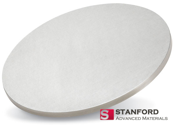
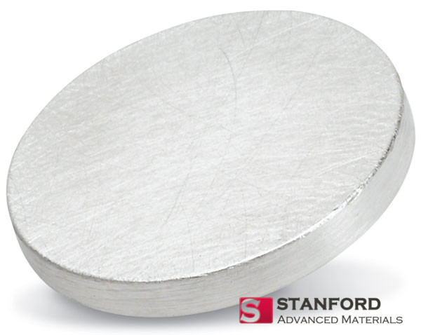
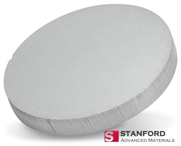
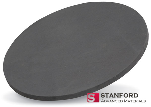
Our Silicon (Si) Rotary Sputtering Targets are engineered for high-volume, uniform deposition of silicon thin films critical for modern electronics and renewable energy. The tubular rotary design maximizes material utilization (>80%) and provides exceptional film thickness uniformity, making it the industry-preferred choice for coating large-area substrates in display, photovoltaic, and semiconductor production lines.
| Material | Silicon (Si) |
| Typical Purity | ≥ 99.9% (3N) to 99.9999% (6N) |
| Form & Shape | Rotary Sputtering Target (Tubular/Cylindrical) |
| Conductivity Type | Intrinsic, P-type (B doped), or N-type (P, As doped) |
| Key Properties | High Deposition Rate | Superior Large-Area Uniformity | Extended Target Life |
| Key Advantage | Delivers significantly higher material utilization and more consistent film properties compared to planar targets, dramatically reducing cost-of-ownership and downtime in high-throughput manufacturing. |
Key Advantage: The rotating cylindrical design ensures even erosion around the circumference, enabling stable, long-duration sputtering runs essential for coating Gen 8.5/10.5+ display glass and large-format photovoltaic panels.
Customization: Purity (3N to 6N), doping type/level, tubular dimensions (OD, ID, Length), grain structure (monocrystalline, polycrystalline), and surface finish are fully customizable for your specific rotary cathode system and process.
Primary Applications: Active and doped silicon layers in Thin-Film Transistor (TFT) arrays for LCD/OLED displays; intrinsic and doped silicon layers in thin-film silicon (a-Si/µc-Si) solar cells; silicon-based passivation and barrier layers in semiconductor devices; silicon nitride/oxide precursor via reactive sputtering.
Comprehensive specifications for high-volume silicon film deposition in display and photovoltaic manufacturing.
| Parameter | Specification / Details |
|---|---|
| Material | Silicon (Si) |
| Purity Grades | Standard: 99.9% (3N), 99.99% (4N), 99.999% (5N), 99.9999% (6N) |
| Crystal Structure | Polycrystalline (Standard) | Monocrystalline (Available) |
| Doping | Intrinsic (Undoped) | P-type (Boron) | N-type (Phosphorus, Arsenic) – Doping level customized |
| Resistivity (Target) | Wide range from <0.01 Ω·cm (heavily doped) to >100 Ω·cm (high purity intrinsic) |
| Density | ≥ 2.33 g/cm³ (>99% of theoretical) |
| Standard Shape | Tubular / Cylindrical Rotary Target |
| Dimensions | Fully Customizable: Outer Diameter (OD), Inner Diameter (ID), Length (L) |
| Typical OD Range | 4″ to 10″ (100 mm to 250 mm) and larger for Gen 10.5+ applications |
| Surface Finish | Precision ground and etched to optimize sputtering performance and minimize initial particulates |
| Bonding / Integration | Designed for direct mounting or bonding to cooling sleeves in standard rotary cathodes |
| Manufacturing Method | Casting of high-purity poly-Si ingots, precision machining, boring, and grinding |
| Sputtering Method | DC Magnetron Sputtering (for conductive doped Si) | RF Magnetron Sputtering (for intrinsic Si) |
| Material Utilization | >80% (Typical for rotary design) |
| Quality Documentation | Certificate of Analysis with resistivity, doping type/level, purity (GDMS), and dimensional report |
Silicon rotary targets are indispensable in the manufacturing of Flat Panel Displays (FPDs):
In the solar industry, silicon rotary targets enable cost-effective production:
Beyond displays and PV, silicon targets serve specialized functions:
The rotary configuration solves key production challenges:
Stanford Advanced Materials employs a precision manufacturing process tailored for large-format rotary targets:
To receive a formal quotation or technical consultation, please provide: