| Material | VSi2 |
| CAS Number | 12039-87-1 |
| Purity | 99.5% |
| Shape | Planar Disc |
The Vanadium Silicide (VSi₂) Target is engineered to deliver exceptional performance in various thin film applications. Composed of vanadium and silicon, VSi₂ boasts a high melting point of approximately 1920°C, ensuring remarkable thermal stability even under stringent processing conditions. Its excellent electrical conductivity makes it a valuable component in electronic and semiconductor devices. Additionally, VSi₂ features a low diffusion coefficient and robust interfacial bonding, enhancing its effectiveness as a barrier or contact layer. Chemically, vanadium silicide is highly resistant to oxidation and corrosion, maintaining a dense and stable surface that can form protective silicon oxide layers upon exposure to air. The material’s mechanical hardness and structural integrity further contribute to its reliability during sputtering and in the resultant thin films.
Related Products: Vanadium Sputtering Target, V, Chromium Vanadium Sputtering Target, Cr/V, N-type Silicon Sputtering Target (N-doped Si), Aluminum Silicon Sputtering Target, Al/Si
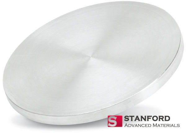
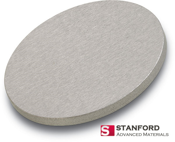
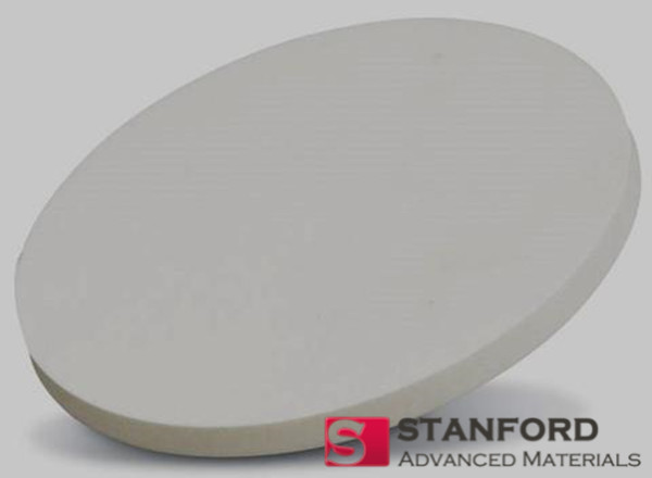
Material: Vanadium Silicide (VSi₂)
Purity: 99.5%
Density: 4.42 g/cm³
Shape: Planar Disc
Note: Specifications are based on theoretical data. For customized requirements and detailed inquiries, please contact us.
Customized sizes are available to meet specific project needs.
The Vanadium Silicide (VSi₂) Target is widely utilized across various high-tech industries due to its unique thermal, electrical, and chemical characteristics:
Our VSi₂ Targets are carefully packaged to ensure their integrity during shipping and storage. Depending on the size, smaller targets are securely placed in polypropylene (PP) boxes, while larger targets are shipped in custom wooden crates. We prioritize customized packaging solutions and use appropriate cushioning materials to provide maximum protection.
Packaging Options:
Q1: Is VSi₂ compatible with both DC and RF sputtering systems?
A1: Yes, Vanadium Silicide targets are suitable for both DC and RF sputtering systems, depending on the specific deposition setup and desired film characteristics.
Q2: How should I store and handle the VSi₂ target?
A2: VSi₂ targets should be stored in a dry, cool environment away from moisture and corrosive substances. Always handle with gloves to prevent contamination of the sputtering surface.
Q3: Can I request a custom composition or doped variant of VSi₂?
A3: Yes, SAM can supply custom compositions or doped variants of vanadium silicide upon request. Please contact us with your specific requirements for a personalized quote.
| Property | VSi₂ Target (Vanadium Silicide) | WSi₂ Target (Tungsten Silicide) | TaN Target (Tantalum Nitride) |
|---|---|---|---|
| Chemical Formula | VSi₂ | WSi₂ | TaN |
| Applications | – Thin-film deposition | – Thin-film deposition | – Hard coatings |
| – Semiconductor devices | – Microelectronics | – Wear-resistant coatings | |
| – High-temperature electronics | – Interconnects, resistors | – Diffusion barriers | |
| – Optical devices | – Semiconductor applications | ||
| Melting Point | ~1850°C | ~3160°C | ~3000°C |
| Density (g/cm³) | ~5.3 | ~6.7 | ~14.1 |
| Electrical Conductivity | Moderate | Low | Low |
| Thermal Conductivity | Moderate to high | High | Moderate to high |
| Hardness | Moderate to high | High | Very high |
| Reactivity | Reacts with oxygen at high temperatures | Stable in air | Stable in air, reactive with strong acids |
| Form | Typically used in sputtering targets and thin films | Common in sputtering for thin films | Used for thin films and coatings |
| Oxidation Resistance | Moderate (forms a protective oxide layer) | High (forms protective oxide layer) | High (forms a stable oxide layer) |
Physical Properties:
Chemical Properties:
Vanadium is a silvery-gray transition metal with atomic number 23, renowned for its strength, corrosion resistance, and ability to form stable compounds. It is extensively used in steel alloys to enhance hardness and durability. Vanadium also plays a crucial role in chemical catalysis and is highly valued in advanced materials for its resistance to oxidation and excellent thermal stability. Its ability to form compounds with desirable conductive and structural properties makes it essential in electronic materials.
Industrial Applications:
Physical Properties:
Chemical Properties:
Silicon is a metalloid with atomic number 14 and is the second most abundant element in the Earth’s crust. It is fundamental to modern electronics, serving as the primary material for semiconductors and integrated circuits. Silicon exhibits excellent semiconducting properties and thermal stability, forming strong bonds with oxygen, which is essential in the production of glass, ceramics, and solar cells. Its versatility and abundance have established it as a cornerstone in the electronics and materials science industries.
Industrial Applications: