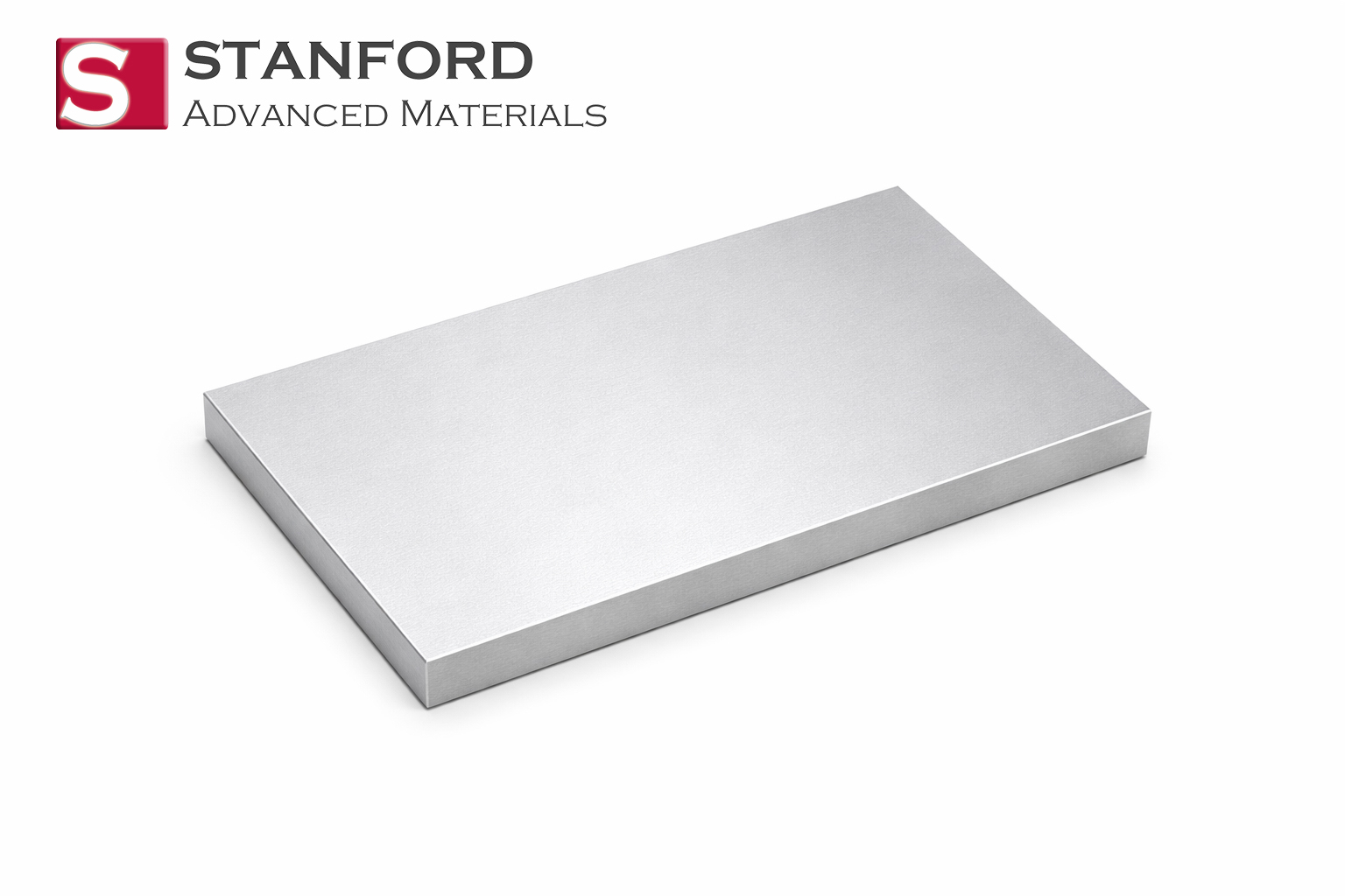
Our Titanium Silicide (TiSi₂) Planar Sputtering Targets are manufactured from the industry-standard C54-phase TiSi₂, a fundamental material in semiconductor metallization. These targets enable the deposition of ultra-low-resistivity films critical for reducing contact resistance and improving device performance in advanced integrated circuits.
| Product Code | ST11217 (Standard Reference) |
| Material | Titanium Disilicide (TiSi₂) |
| Typical Purity | ≥ 99.9% |
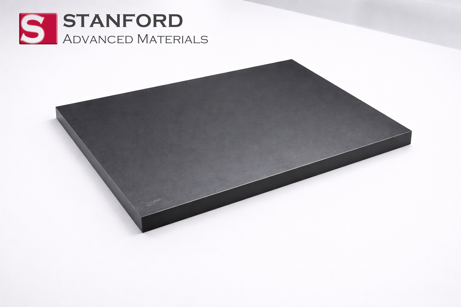
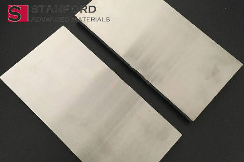
| Form & Shape | Planar Sputtering Target (Rectangular/Disc) |
| Crystal Phase | C54 (Low-Resistivity Orthorhombic Phase) |
| Key Advantage | Enables formation of the lowest resistivity silicide films (~13-20 µΩ·cm) essential for high-speed semiconductor contacts and interconnects in sub-micron technologies. |
Key Advantage: Provides the optimal material source for forming TiSi₂ contacts through the self-aligned silicide (salicide) process, significantly reducing parasitic resistance in source/drain and gate regions.
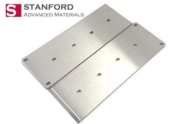
Customization: Stoichiometry (Ti:Si ratio), purity, dimensions (thickness, width, length), and bonding configurations are fully customizable for specific process integration requirements.
Primary Applications: Source/drain and gate contacts in CMOS transistors; local interconnects in integrated circuits; low-resistance electrodes for sensors and MEMS devices; diffusion barrier layers in advanced metallization schemes.
Comprehensive specifications for semiconductor process integration and advanced contact engineering.
| Parameter | Specification / Details |
|---|---|
| Material | Titanium Disilicide (TiSi₂) |
| Crystal Phase (Target) | Primarily C54 Orthorhombic Phase (Optimized for low-resistivity film formation) |
| Typical Purity | ≥ 99.9% (Metal Basis) |
| Stoichiometry | Ti:Si ≈ 1:2 (Atomic) | Custom ratios available for process optimization |
| Density | ~4.13 g/cm³ (Theoretical for C54-TiSi₂) |
| Melting Point | Approx. 1500 °C |
| Electrical Resistivity (Film) | ~13 – 20 µΩ·cm (For optimal C54-phase films after proper annealing) |
| Formation Temperature | C54 phase typically forms at 700-900°C during RTP annealing |
| Standard Shape | Planar – Rectangular, Circular (Disc) |
| Dimensions | Fully Customizable (Thickness, Width, Length, Diameter) |
| Surface Finish | Precision ground and polished for uniform sputtering performance |
| Bonding Option | Available bonded to Cu or Al backing plates using In, Elastomer, or specialized bonding |
| Manufacturing Method | Powder metallurgy with controlled sintering to achieve phase purity and density |
| Quality Documentation | Certificate of Analysis with XRD phase identification and compositional data |
Titanium Silicide has been the workhorse material for contact formation in semiconductor manufacturing for decades:
TiSi₂ offers specific benefits for semiconductor integration:
While largely succeeded by CoSi₂ and NiSi at the most advanced nodes, TiSi₂ remains important for:
Stanford Advanced Materials ensures target quality through stringent controls:
To receive a formal quotation or technical consultation, please provide: