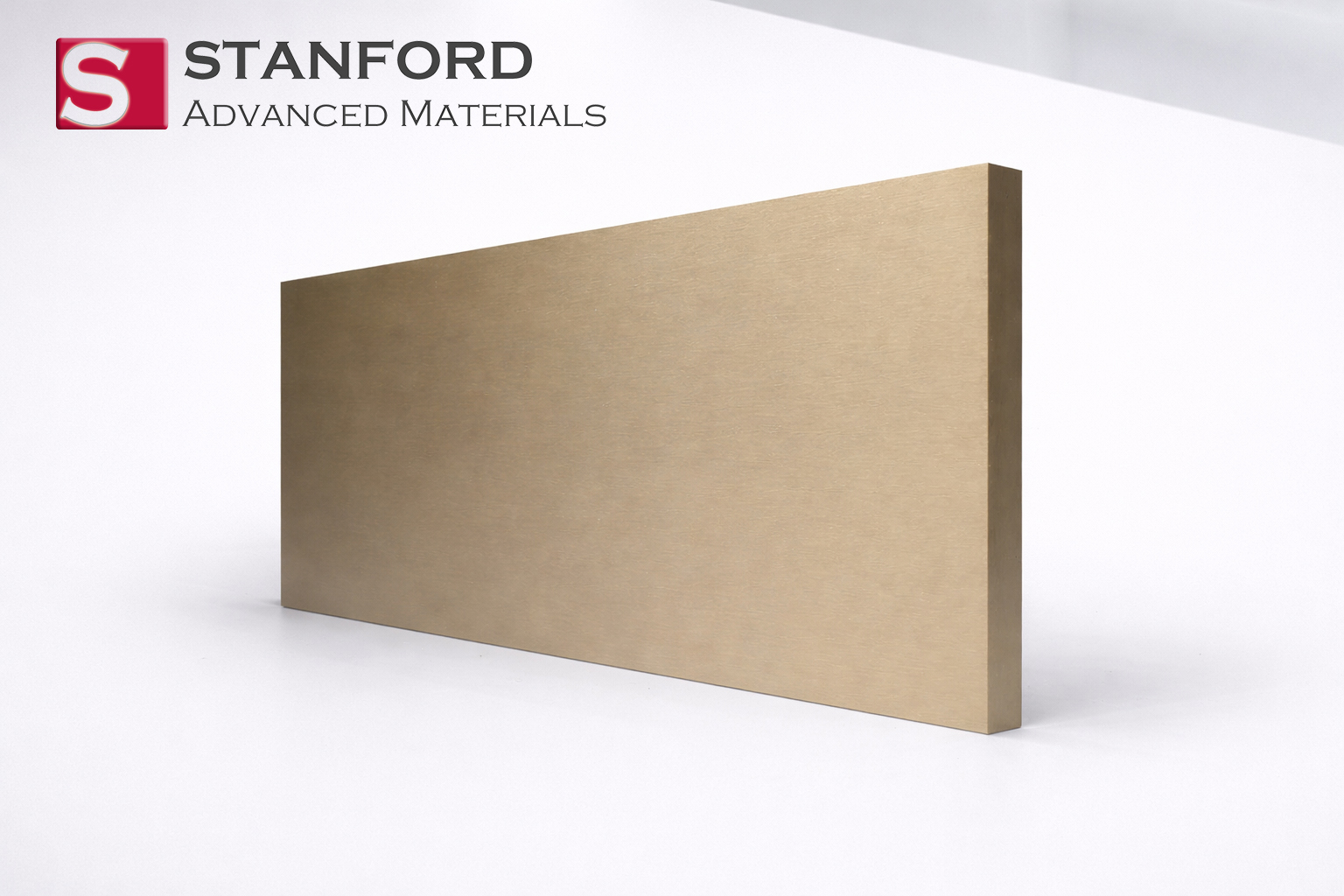
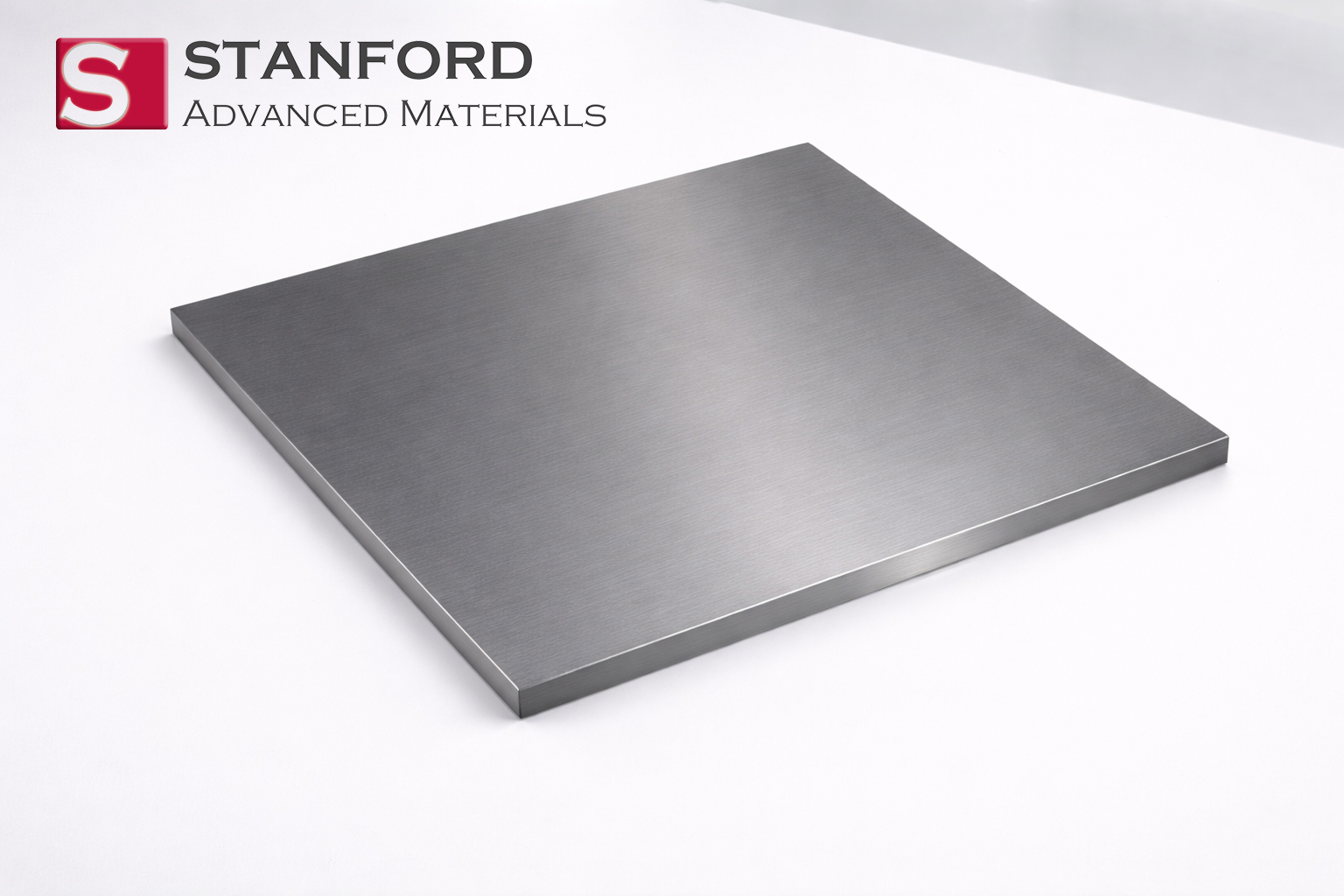
Our Tantalum Silicide (TaSi₂) Planar Sputtering Targets are engineered from the well-defined TaSi₂ intermetallic phase, a critical material in semiconductor metallization. These targets enable the deposition of conductive films with an optimal balance of low resistivity, excellent thermal stability, and strong adhesion—making them indispensable for advanced microelectronic device fabrication.
| Product Code | ST11216 (Standard Reference) |
| Material | Tantalum Disilicide (TaSi₂) |
| Typical Purity | ≥ 99.9% |
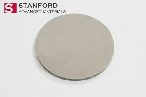
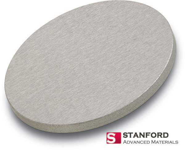
| Form & Shape | Planar Sputtering Target (Rectangular/Disc) |
| Key Properties | Low Resistivity (~35-50 µΩ·cm) | High Thermal Stability | Excellent Diffusion Barrier |
| Key Advantage | Provides a stable, conductive thin film source for gate electrodes and local interconnects in CMOS technology, with compatibility to high-temperature processing steps. |
Key Advantage: Enables deposition of conductive films that maintain stability and low resistance after high-temperature annealing, which is critical for integrating with self-aligned silicide (salicide) processes in semiconductor manufacturing.
Customization: Composition ratio (Ta:Si), purity, dimensions, and bonding options are fully customizable to match specific integration schemes and device requirements.
Primary Applications: Gate electrode and local interconnect material in CMOS devices; diffusion barrier/contact layer for DRAM and advanced logic; conductive coating for MEMS and high-temperature sensors.
Detailed specifications tailored for semiconductor process integration and advanced metallization research.
| Parameter | Specification / Details |
|---|---|
| Material | Tantalum Disilicide (TaSi₂) |
| Crystal Phase | Hexagonal (C40 structure) – The stable, low-resistivity phase for thin-film applications |
| Typical Purity | ≥ 99.9% (Metal Basis) |
| Composition Ratio | Ta:Si ≈ 1:2 (Atomic) | Custom ratios (e.g., Si-rich or Ta-rich) available |
| Density | ~9.14 g/cm³ (Theoretical) |
| Melting Point | Approx. 2200 °C |
| Electrical Resistivity (Bulk) | ~35 – 50 µΩ·cm (Film resistivity depends on deposition and annealing conditions) |
| Thermal Stability | Stable in contact with Si up to ~1000°C, forms low-resistance ohmic contacts |
| Standard Shape | Planar – Rectangular, Circular (Disc) |
| Dimensions | Fully Customizable (Thickness, Width, Length, Diameter) |
| Surface Finish | Fine-ground and polished for uniform sputtering and minimal particulate generation |
| Bonding Option | Available bonded to Cu or Al backing plates using In, Elastomer, or solder |
| Manufacturing Method | Arc Melting / Powder Metallurgy with controlled sintering to ensure phase purity |
| Quality Documentation | Certificate of Analysis (CoA) with phase verification (XRD) and composition data |
Tantalum Disilicide has been a cornerstone material in semiconductor technology due to its unique combination of properties:
The performance of TaSi₂ films critically depends on achieving the correct crystalline phase:
DC magnetron sputtering from conductive TaSi₂ targets is the standard deposition method:
Stanford Advanced Materials implements rigorous controls to ensure target performance:
To receive a formal quotation or technical consultation, please provide: