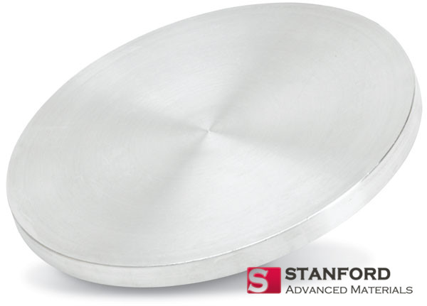
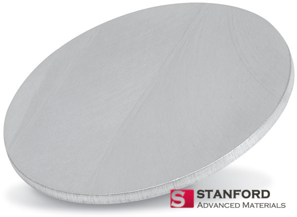
Our High-Purity Silicon (Si) Planar Sputtering Targets are essential for depositing intrinsic, doped, or compound silicon films in semiconductor device fabrication, photovoltaic research, and infrared (IR) optics. The choice between monocrystalline and polycrystalline structure, along with stringent impurity control, directly determines the electrical and optical properties of the deposited layer.
| Material | Silicon (Si) |
| Purity | ≥ 99.99% (4N) Standard |
| Available Structure | Monocrystalline, Polycrystalline |
| Form | Planar Sputtering Target |
Key Advantage: Exceptionally low levels of dopants (B, P, As) and metallic impurities ensure predictable electrical resistivity and optical transmission in the deposited films, critical for research and precision manufacturing.
Customization: Purity (up to 99.999%), dimensions, crystal orientation (<100>, <111> for monocrystalline), and bonding to various backing plates fully customizable.
Typical Applications: Thin films for semiconductor gate electrodes, photovoltaic absorbers (a-Si, μc-Si), IR anti-reflection coatings, and silicon-based compound layers (e.g., SiOx, SiNx via reactive sputtering).
For detailed evaluation and procurement.
| Parameter | Specification / Typical Value |
|---|---|
| Material | Silicon (Si) |
| Purity (Standard) | ≥ 99.99% (4N) |
| Available Structure | Monocrystalline (CZ/FZ), Polycrystalline |
| Resistivity (Intrinsic) | > 1000 Ω·cm (High-Purity Grade) |
| Density | 2.329 g/cm³ |
| Band Gap | 1.12 eV (300K) |
| Thermal Conductivity | ~150 W/(m·K) |
| Standard Shape | Rectangular Planar |
| Dimensions | Fully Customizable |
| Sputtering Method | DC or RF Magnetron Sputtering |
| Bonding Options | Indium, Elastomer, or high-temperature solders to Cu/Mo backing plates |
| Certification | Certificate of Analysis (CoA) with GDMS/ICP-MS data for key impurities (B, P, metals) |
Silicon targets are used beyond bulk wafer substrates to deposit functional thin films:
Silicon is a brittle semiconductor, requiring specific handling:
For semiconductor-grade silicon targets, we provide detailed impurity analysis using Glow Discharge Mass Spectrometry (GDMS) to quantify trace elements at ppb levels. Special attention is paid to electrically active impurities like Boron (B) and Phosphorus (P), which drastically alter film resistivity. For monocrystalline targets, orientation and crystallographic defects are also characterized.
Specify Your Silicon Film Requirements
To recommend the optimal target, please provide: