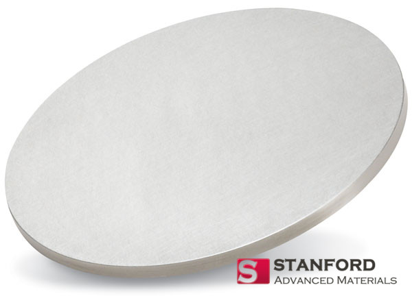
Our High-Purity Lead (Pb) Planar Sputtering Targets are engineered for specialized research and development applications, primarily in the fields of low-temperature superconductivity and infrared (IR) photodetectors. Ultra-high purity is critical to minimize impurities that can degrade the performance of these sensitive thin-film devices.
| Material | Lead (Pb) |
| Purity | ≥ 99.99% (4N) Standard |
| Key Property | Superconducting Transition Temperature (Tc = 7.2 K) |
| Form | Planar Sputtering Target |
Key Advantage: Exceptionally low levels of metallic and gaseous impurities ensure the deposited lead films achieve optimal superconducting and electronic properties for fundamental physics and device research.
Customization: Purity (up to 99.999%), dimensions (thickness, length, width), and bonding options fully customizable.
Typical Applications: Thin films for superconducting quantum interference devices (SQUIDs), Josephson junctions, IR photodetectors (e.g., PbSe, PbTe precursors), and specialized X-ray/radiation shielding coatings.
For detailed evaluation and procurement (Standard Reference: ST11206).
| Parameter | Specification / Typical Value |
|---|---|
| Material | Lead (Pb) |
| Purity (Standard) | ≥ 99.99% (4N) |
| Available Purity | 99.99%, 99.999% |
| Density | ≥ 11.34 g/cm³ |
| Superconducting Tc | 7.2 K (High-Purity Bulk) |
| Melting Point | 327.5 °C |
| Thermal Conductivity | 35.3 W/(m·K) |
| Standard Shape | Rectangular Planar |
| Dimensions | Fully Customizable |
| Sputtering Method | DC Magnetron (Low Power Recommended) |
| Bonding Options | Low-temperature bonding to backing plates available |
| Certification | Certificate of Analysis (CoA) with GDMS/ICP-MS data provided |
Lead is a classic low-temperature superconductor. High-purity lead thin films are essential for fabricating:
The superconducting transition temperature (Tc) and critical current are highly sensitive to impurities and film morphology, making target purity and process control paramount.
Lead chalcogenides (PbS, PbSe, PbTe) are important semiconductors for mid- and long-wavelength infrared detection. Sputtering from a high-purity lead target in a reactive sulfur, selenium, or tellurium atmosphere is one method to deposit these compound films for IR sensors, thermal imaging, and spectroscopic applications.
Lead is a soft, low-melting-point metal with specific handling requirements:
For lead intended for superconducting applications, trace impurity analysis is critical. We utilize Glow Discharge Mass Spectrometry (GDMS) or Inductively Coupled Plasma Mass Spectrometry (ICP-MS) to provide parts-per-billion (ppb) level quantification of elements like Fe, Cu, Ag, and Bi, which can severely degrade superconducting performance. This high-sensitivity certification differentiates our research-grade targets.
Get a Formal Quote or High-Sensitivity CoA
For research applications where purity is critical, please provide: