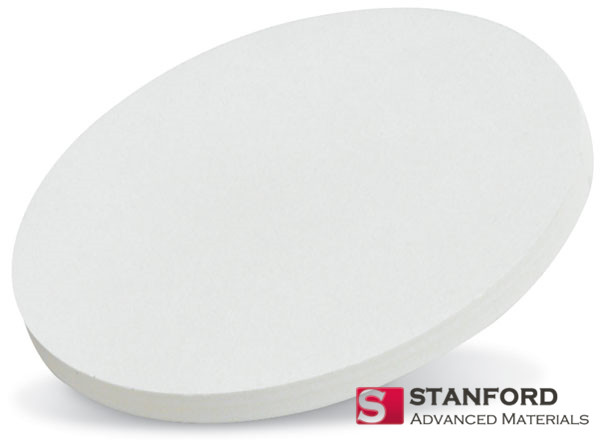
Our Indium Tin Oxide (ITO) Rotary Sputtering Targets are engineered to meet the rigorous demands of large-area, high-throughput coating processes. With the standard 90 wt.% In₂O₃ / 10 wt.% SnO₂ composition and high density, they enable the efficient and uniform deposition of high-quality transparent conductive films—the backbone of modern displays, touch interfaces, and thin-film photovoltaics.
| Material | Indium Tin Oxide (ITO) |
| Standard Composition | In₂O₃ : SnO₂ = 90 : 10 by weight (Standard) |
| Purity | ≥ 99.99% (4N) |
| Form | Rotary Sputtering Target (Tubular) |
Key Advantage: High density (≥95% T.D.) and homogeneous microstructure ensure stable, low-particle sputtering with excellent film uniformity, high transmittance, and low resistivity over the entire target life.
Customization: Composition (e.g., 95/5), density, tube dimensions (OD, ID, Length), and bonding fully customizable.
Typical Applications: Transparent electrodes for LCD/OLED/QLED displays, touch sensors (touch panels, on-cell touch), thin-film solar cells (heterojunction, perovskite), and EMI shielding coatings.
For detailed evaluation and procurement (Standard Reference: ST11192).
| Parameter | Specification / Typical Value |
|---|---|
| Material | Indium Tin Oxide (ITO) |
| Standard Composition | In₂O₃ (90 wt.%), SnO₂ (10 wt.%) |
| Available Compositions | 95/5, 90/10, 85/15 (Custom ratios available) |
| Purity | ≥ 99.99% (on oxide basis) |
| Density | ≥ 7.13 g/cm³ (Typically >95% Theoretical Density) |
| Relative Density | ≥ 95% |
| Resistivity (Target) | High (Insulating) |
| Standard Shape | Tubular (Rotary Target) |
| Key Dimensions | Custom OD, ID, Length (for Gen 2 to Gen 10.5+ lines) |
| Color | Yellowish-green |
| Sputtering Method | DC (with specific process gas), Pulsed-DC, RF |
| Bonding/Integration | Typically bonded to Cu or SS backing tube for cooling |
| Certification | Certificate of Analysis (CoA) provided |
1. The Dominant TCO for Optoelectronics
ITO remains the industry benchmark for transparent conductive films due to its optimal balance of high optical transmittance (>90% in visible spectrum) and low electrical resistivity (as low as 1-2 x 10⁻⁴ Ω·cm). The 90/10 composition offers the best trade-off between conductivity, etching characteristics, and cost for most display applications.
2. Why Density and Microstructure are Critical
For ITO targets, achieving high density (>95% of theoretical) is paramount. High density:
3. Rotary Design: Engineered for Scale and Uniformity
In display fabs (Gen 6 to Gen 10.5), rotary targets are the undisputed standard for ITO deposition because they:
4. Process Considerations
ITO is a ceramic material and is typically sputtered in a reduced-pressure argon-oxygen mixture. The exact gas ratio and power mode (DC, pulsed-DC) are tuned to achieve the desired film resistivity and stress without inducing target poisoning or arcing.
Our ITO targets are produced via hot pressing (HP) or sintering of high-purity oxide powders under controlled atmospheres. Each batch is characterized for:
Get a Formal Quote or Technical Datasheet
For production-scale ITO targets, please provide detailed specifications: