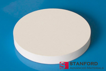
Our Cadmium Sulfide (CdS) Planar Sputtering Targets are engineered from high-purity compound semiconductor materials, providing a reliable source for depositing n-type window or buffer layers essential in thin-film photovoltaics (CIGS, CdTe) and various optoelectronic devices.
| Material | Cadmium Sulfide (CdS) |
| Purity | ≥ 99.99% (4N) |
| Crystal Structure | Hexagonal (Wurtzite) or Cubic (Zinc Blende) |
| Form | Planar Sputtering Target |
Key Advantage: High stoichiometric control and purity ensure deposited films exhibit consistent optical bandgap (~2.42 eV), excellent n-type conductivity, and uniform morphology for device performance.
Customization: Purity, dimensions (thickness, length, width), and bonding options fully customizable.
Typical Applications: Buffer/window layers for CIGS and CdTe solar cells, photoconductive detectors, thin-film transistors (TFTs), and II-VI semiconductor heterostructure research.
For detailed evaluation and procurement (Standard Reference: ST11174)
| Parameter | Specification / Typical Value | Notes / Process Relevance |
|---|---|---|
| Material | Cadmium Sulfide (CdS) | A direct bandgap II-VI compound semiconductor. |
| Purity (Standard) | ≥ 99.99% (4N) | Minimizes impurities that act as recombination centers, critical for photovoltaic efficiency and detector response. |
| Stoichiometry | Cd:S ≈ 1:1 (Controlled) | Deviations can alter conductivity type and optical absorption; precise control is maintained. |
| Density | ≥ 4.35 g/cm³ (>95% T.D.) | High density is crucial for reducing porosity, arcing, and achieving high-quality, adherent films. |
| Crystal Structure | Primarily Hexagonal (Wurtzite) | The stable phase at room temperature; cubic phase available upon request. |
| Band Gap (Material) | ~2.42 eV (Direct, @300K) | Defines the optical absorption edge; ideal for window layers in tandem solar cells. |
| Standard Shape | Rectangular (e.g., 150x150x10 mm) | Circular and other custom geometries available. |
| Dimensions | Fully Customizable | Thickness, length, and width tailored to your chamber. |
| Resistivity (Target) | High (Insulating/Semiconducting) | Requires RF or Pulsed-DC sputtering methods. |
| Sputtering Method | RF Magnetron (Standard), Pulsed-DC | Recommended for stable deposition of compound semiconductor materials. |
| Bonding Options | Bonding to Mo, Cu, or SS backing plates available | Enhances thermal conductivity and mechanical stability during sputtering. |
| Certification | Certificate of Analysis (CoA) provided | Includes purity, stoichiometry (via ICP), and phase analysis (XRD). |
1. The Critical Role of CdS in Thin-Film Photovoltaics
In CIGS (Copper Indium Gallium Selenide) and CdTe (Cadmium Telluride) solar cells, a thin layer of n-type CdS is traditionally used as the heterojunction partner/buffer layer on the p-type absorber. Its function is multifaceted: it forms a favorable band alignment for charge separation, protects the absorber during subsequent processing, and allows high-energy photons to pass through. The purity and stoichiometry of our target directly influence the interface quality and, consequently, the cell’s open-circuit voltage and fill factor.
2. Material Considerations for Sputtering
CdS is a compound semiconductor with relatively high resistivity. Therefore, RF sputtering is the most common and reliable technique to avoid charging and achieve stoichiometric film transfer. Our targets are processed via hot pressing or chemical vapor deposition (CVD) of high-purity precursors to achieve high density, phase purity, and excellent stoichiometric control, which are essential for reproducible film properties.
3. Application-Specific Guidance
Each CdS target is comprehensively characterized. X-ray Diffraction (XRD) confirms the crystal phase and absence of secondary phases (e.g., CdO, S). Inductively Coupled Plasma (ICP) analysis verifies elemental purity and Cd:S ratio. Microstructural analysis ensures density and absence of cracks or voids. This data is included in the provided CoA.
Get a Formal Quote or Technical Datasheet
To discuss your CdS film requirements, please provide: