| Chemical Formula | Ga2S3 |
| Catalog No. | ST0965 |
| CAS Number | 12024-22-5 |
| Purity | 99.9%, 99.95%, 99.99%, 99.995%, 99.999% |
| Shape | Discs, Plates, Column Targets, Step Targets, Custom-made |
Our Gallium Sulfide (Ga₂S₃) Sputtering Targets provide a high-quality source for depositing thin films of this wide bandgap (~3.0-3.4 eV) semiconductor, which exhibits promising properties for ultraviolet photodetectors, phosphor hosts, and as a component in complex chalcogenide glasses for photonics and memory applications.
Gallium (III) Sulphide Sputtering Targets have good uniformity and controllability during thin film deposition, supporting the formation of reliable films on substrates. Gallium Sulphide excels in optics, with transmission and absorption properties that make it widely used in optical coatings and optical devices. As a semiconductor material, Gallium Sulphide shows electrical properties that make it suitable for the preparation of electronic devices. Gallium Sulphide is stable in certain environments, which affects its long-term stability in different applications.
Related Product: Gallium (III) Selenide Sputtering Target, CIGS Copper Indium Gallium (III) Sulphide Sputtering Target
| Compound Formula | Ga2S3 |
| Molecular Weight | 235.64 |
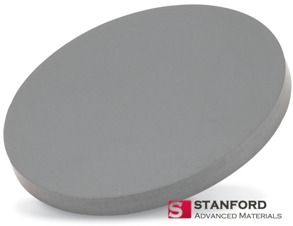
| Appearance | Silver Grey Target |
| Melting Point | 1255 °C |
| Density | 3.65 g/cm3 |
| Available Sizes | Dia.: 1.0″, 2.0″, 3.0″, 4.0″, 5.0″, 6.0″
Thick: 0.125″, 0.250″ |
Our Gallium (III) Sulphide Sputtering Target is carefully handled during storage and transportation to preserve the quality of our products in their original condition.
SAM’s Gallium (III) Sulphide Sputtering Target is available in various forms, purities, and sizes. We specialize in producing high-purity physical vapour deposition (PVD) materials with the highest possible density and smallest possible average grain sizes for use in semiconductor, chemical vapour deposition (CVD), and physical vapour deposition (PVD) display and optical applications.