| Catalog No. | CY2175 |
|---|---|
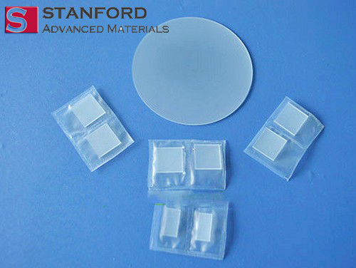
| Material | SiC |
| Thickness | 330 um ~ 350 um |
| Conductive Type | N – type / Semi-insulating |
| Diameter | Ø 2″ / Ø 3″ / Ø 4″ |
| Polytype | 4H / 6H |
| Resistivity ( SI ) | > 1E5 ohm-cm |
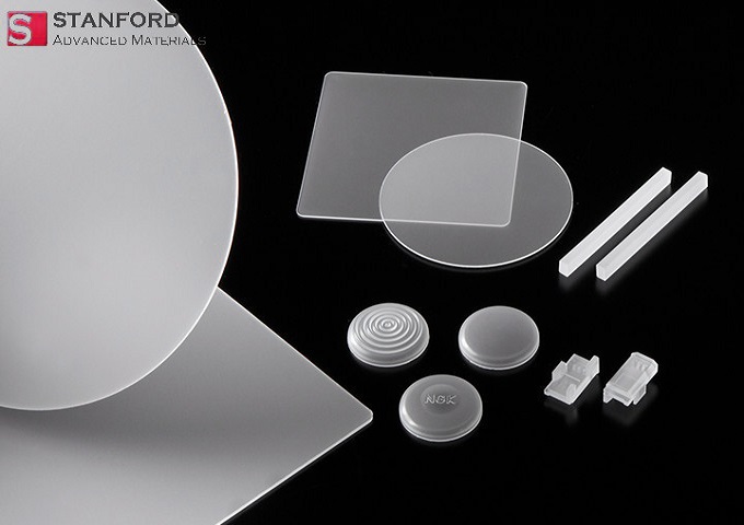
Stanford Advanced Materials (SAM) is a global manufacturer of Silicon Carbide Wafer. With our rich experience and knowledge in the wafer industry, you can be confident in making SAM your first choice.
As a next-generation semiconductor material, silicon carbide wafer has unique electrical properties and excellent thermal properties. The sic-based device has been used for short-wavelength optoelectronic, high temperature, radiation resistant applications. In the applications of high power and high temperature, SiC wafer is more suitable compared to the silicon wafer and GaAs wafer.
|
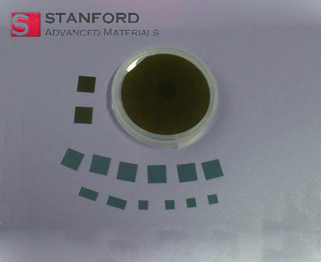
Polytype |
4H / 6H |
|
Diameter |
Ø 2″ / Ø 3″ / Ø 4″ |
|
Thickness |
330 um ~ 350 um |
|
Orientation |
On axis <0001> / Off axis <0001> off 4° |
|
Conductivity |
N – type / Semi-insulating |
|
Dopant |
N2 ( Nitrogen ) / V ( Vanadium ) |
|
Resistivity ( 4H-N ) |
0.015 ~ 0.03 ohm-cm |
|
Resistivity ( 6H-N ) |
0.02 ~ 0.1 ohm-cm |
|
Resistivity ( SI ) |
> 1E5 ohm-cm |
|
Surface |
CMP polished |
|
TTV |
≤ 15 um |
|
Bow / Warp |
≤ 25 um |
|
Grade |
Production grade / Research grade |
|
Polytype |
6H-SiC |
4H-SiC |
|
Crystal stacking sequence |
ABCABC |
ABCB |
|
Lattice parameter |
a=3.073A , c=15.117A |
a=3.076A , c=10.053A |
|
Band-gap |
3.02 eV |
3.27 eV |
|
Dielectric constant |
9.66 |
9.6 |
|
Refraction Index |
n0 =2.707 , ne =2.755 |
n0 =2.719 ne =2.777 |
Silicon carbide wafers have the following applications:
– High-frequency device
– High power device
– GaN epitaxy device
– High-temperature device
– Optoelectronic device
– Light-emitting diode
Submit your review | |
Just what I needed for my project, fast shipping and no hassles.