| Catalog No. | CY2173 |
|---|---|
| Material | Al2O3 |
| Thickness | 430mm, 0.5mm, 1mm |
| Diameter | Ø 1″ /Ø 2″ / Ø 3″ / Ø 4″/ Ø6″ |
| Thermal Conductivity | 46 W/mk |
| Dielectric constant | 11.58 |
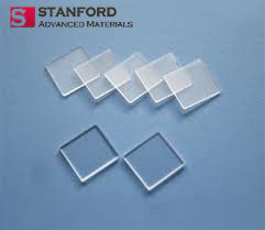
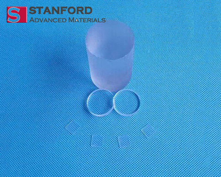
Stanford Advanced Materials (SAM) produces any diameters of the sapphire wafer from 1’’ (25.4 mm) to 5’’ (152.4mm) in order to provide the most flexibility as possible. We can offer complete orientation options including C plane, A plane, R plane and M plane.
Comparing to other wafers, the sapphire wafer has many unique features such as high strength, anti-corrosion, anti-abrasion, good thermal conductivity, and good electrical isolation. Due to its excellent mechanical and chemical characteristics, the sapphire wafer plays an important role in the optoelectronics industry and widely used in precision mechanical parts and vacuum equipment.
|
Growth |
Kyroplous |
|
Diameter |
Ø 1″ / Ø 2″ / Ø 3″ / Ø 4″/ Ø 6″ |
|
Size |
10 x 10 / 20 x 20 / 50 x 50 / 100 x 100 mm |
|
Thickness |
0.43 mm / 0.5 mm / 1 mm |
|
Surface |
one side / two sides epi polished |
|
Roughness |
Ra ≤ 5 A |
|
Package |
Single wafer container or Ampak cassette |
|
Chemical formula |
Al2O3 |
|
Crystal structure |
Hexagonal |
|
Lattice constant |
4.77 A |
|
Hardness |
9 |
|
Thermal conductivity |
46 W / mk |
|
Dielectric constant |
11.58 |
|
Refractive index |
1.768 |
Sapphire wafers have been used in:
– High-frequency device
– High power device
– GaN epitaxy device
– High-temperature device
– Optoelectronic device
– Light-emitting diode
Submit your review | |
Worked perfectly for my summer camp project. Good value.