Sputtering Target")
Chemical Formula: Ti2O3
Catalog Number: ST0195
CAS Number: 1344-54-3
Purity: 99.9%
Shape: Discs, Plates, Column Targets, Step Targets, Custom-made
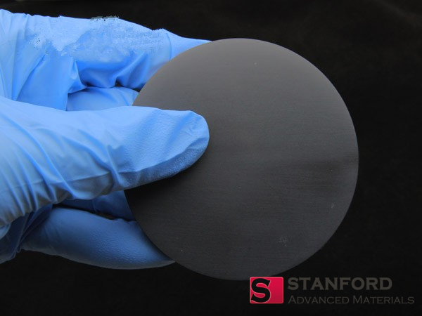
The titanium trioxide sputtering target is available in various forms, purities, sizes, and prices. Stanford Advanced Materials (SAM) offers high-quality titanium trioxide sputter targets at the most competitive prices.
Titanium trioxide sputtering target from Stanford Advanced Materials is an oxide sputtering material containing Ti and O.
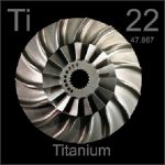 Titanium is a chemical element that originated from Titans, the sons of the Earth goddess of Greek mythology. It was first mentioned in 1791 and observed by W. Gregor. The isolation was later accomplished and announced by J. Berzelius. “Ti” is the canonical chemical symbol of titanium. Its atomic number in the periodic table of elements is 22 with a location at Period 4 and Group 4, belonging to the d-block. The relative atomic mass of titanium is 47.867(1) Dalton, the number in the brackets indicating the uncertainty.
Related Product: Titanium Sputtering Target
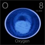 Oxygen is a chemical element that originated from the Greek ‘oxy’ and ‘genes’ meaning acid-forming. It was first mentioned in 1771 and observed by W. Scheele. The isolation was later accomplished and announced by W. Scheele. “O” is the canonical chemical symbol of oxygen. Its atomic number in the periodic table of elements is 8 with a location at Period 2 and Group 16, belonging to the p-block. The relative atomic mass of oxygen is 15.9994(3) Dalton, the number in the brackets indicating the uncertainty.
Related Product: Oxide Ceramic Sputtering Target
| Material Type | Titanium Trioxide |
| Compound Formula | Ti2O3 |
| Molecular Weight | 143.73 g/mol |
| Appearance | Violet black solid |
| Melting Point | 2,130° C (3,866° F) |
| Type of Bond | Indium |
Indium Bonding is available for Titanium Trioxide Sputtering Target. Stanford Advanced Materials is devoted to machining standard backing plates and working together with the Taiwan Bonding Company for providing bonding services. For questions about target bonding materials, methods and services, please click here.
Our Titanium Trioxide Sputtering Target is clearly tagged and labeled externally to ensure efficient identification and quality control. Great care is taken to avoid any damage which might be caused during storage or transportation.
SAM specializes in producing high purity Titanium Trioxide Sputtering Target with the highest possible density and smallest possible average grain sizes for use in semiconductor, chemical vapor deposition (CVD) and physical vapor deposition (PVD) display and optical applications. Please send us an inquiry for the current prices of the sputtering targets and other deposition materials that are not listed.
Submit your review | |
Value for money, this is a solid purchase.