| Catalog No. | IN2270 |
|---|---|
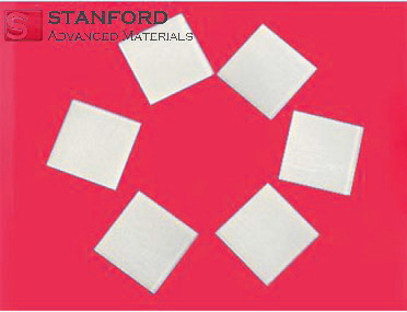
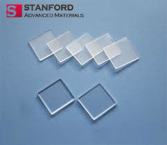
| Material | InSb |
| Thickness | 500 um |
| Conductive Type | N – type |
| Diameter | Ø 2″ Ø 3″ |
Stanford Advanced Materials (SAM) provides a wide range of compound wafers including Indium Antimonide Wafer, Gallium Arsenide Wafer, Gallium Phosphide Wafer and Gallium Antimony Wafer.
Indium antimonide wafer is made of a crystalline compound made from the elements indium (In) and antimony (Sb). It is a narrow-gap semiconductor material from the III-V group used in infrared detectors, including thermal imaging cameras, FLIR systems, infrared homing missile guidance systems, and infrared astronomy. The indium antimonide detectors are sensitive between 1–5 µm wavelengths. Indium antimonide was a very common detector in the old, single-detector mechanically scanned thermal imaging systems. Another application is as a terahertz radiation source as it is a strong photo-Dember emitter.
|
Growth |
LEC |
|
Diameter |
Ø 2″ / Ø 3″ |
|
Thickness |
500 um – 625 um |
|
Orientation |
(100)+/- 0.5° |
|
Off orientation |
Off 2° to 10° |
|
Surface |
One side polished or two sides polished |
|
Flat options |
EJ or SEMI. Std . |
|
Mobility |
(5.0-3.5)E5 cm2/Vs |
|
EPD |
<= 200 cm-2 |
|
Grade |
Epi polished grade / mechanical grade |
|
Package |
Single wafer container |
Indium antimonide wafer has the following applications:
– Solar photovoltaic
– Integrated circuits
– Transistor
Submit your review | |
Product looks really good in person rather than a photo.