Specifications of Gallium Arsenide Wafers
Introduction
Gallium Arsenide (GaAs) wafers are an essential component in the production of high-performance electronic devices, and they have specific specifications that must be met to ensure their effectiveness. In this article, we will discuss the key specifications of GaAs wafers so that you can have a further understanding of this useful material.
What Are Gallium Arsenide Wafers?
Gallium arsenide wafers are a kind of semiconductor that is commonly used in high-frequency electronic equipment and optical devices, including light-emitting diodes, laser diodes, and high electron mobility transistors. GaAs wafers stand out for the following features.
- Electron Mobility: First of all, electrons move much faster inside gallium arsenide wafers. This property makes GaAs wafers extremely useful for manufacturing high-speed telecommunication devices and high-frequency electronic equipment, such as high-frequency transistors and amplifiers.
- Direct Bandgap: GaAs wafers have a direct bandgap, so electrons and photons can pass through them quickly and with ease, and they are applied to a wide range of applications, such as laser diodes, solar cells, etc.
- Resistivity: GaAs wafers are more resistive than silicon and other traditional wafers. The high dielectric constant makes GaAs wafers popular materials for substrates with natural isolation.
Specifications of Gallium Arsenide Wafers
Stanford Advanced Materials (SAM) provides GaAs wafers that meet the following specifications. You can select suitable ones for your business and research.
Size & Thickness
The first specification of GaAs wafers is their size. Their most common size is 2 inches in diameter, but they can also come in 3, 4, 6, and 8-inch sizes. The thickness of GaAs wafers ranges from 350 microns to 625 microns, depending on the specific application. There are GaAs wafers of 2, 3, 4 inches, and other customized sizes available on https://www.sputtertargets.net/, and their thickness is between 350µm and 625µm.
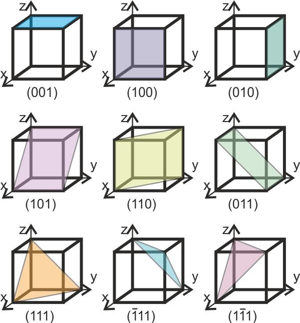
Crystal Orientation
Another significant specification of GaAs wafers is their crystal orientation, which is presented by Miller indices. The two most common orientations for GaAs wafers are (100) and (111) orientations and they affect the electrical features of wafers. The (100) orientation is the most common type, and it is used in the production of high-frequency and power electronics devices, while the (111) orientation is employed in the production of optoelectronic devices such as photovoltaic cells and light-emitting diodes (LEDs). You can also find (110) on our website.
–Conductivity Type
GaAs wafers can be either n-type or p-type conductivity depending on the impurities that are introduced during the manufacturing process. N-type GaAs wafers have excess electrons, while p-type GaAs wafers have a deficiency of electrons. The type of conductivity is crucial for high-frequency devices because these devices’ performance is affected by the conductivity type. Both n-type and p-type are available at https://www.sputtertargets.net/.
–Carrier concentration
Carrier Concentration is another significant specification that affects the electrical properties of GaAs wafers. The carrier concentration is measured in units of cm^-3 and refers to the number of free electrons or holes per cubic centimeter. It affects the conductivity of the wafer, and therefore its performance in electronic devices.
–Resistivity
The sixth specification of GaAs wafers is their resistivity. The resistivity of GaAs wafers is a measure of their ability to resist the flow of electrical current. Low resistivity is essential for the efficient flow of electrical current in electronic devices.
–Surface Quality
The fifth specification of GaAs wafers is their surface quality, which is measured in terms of roughness, scratches, and defects. A high-quality surface is essential for the efficient operation of electronic devices as it minimizes signal loss and interference.
For more information, please check the table below.
Table 1. The Specifications of GaAs Wafers
| Material | GaAs Wafers |
| Diameter | Ø 2″ / Ø 3″ / Ø 4″ |
| Thickness | 350µm – 625µm |
| Crystal Orientation | <100> / <111> / <110> or others |
| Conductive Type | P-type / N-type / Semi-insulating |
| Carrier Concentration | 1E17 ~ 5E19 cm-3 |
| Surface Polishing | One side polished or two sides polished |
Conclusion
Overall, GaAs wafers have specific specifications that must be met to ensure their efficacy in the production of high-performance electronic devices. These specifications include size, thickness, crystal orientation, conductivity type, carrier concentration, surface quality, and resistivity. Understanding and meeting these specifications is critical in the production of high-quality GaAs wafers that can be used in a broad range of electronic devices.
Stanford Advanced Materials (SAM) has rich experience in the manufacturing of quality gallium arsenide wafers. Please send us an inquiry if you are interested.
Reference:
[1] Waeselmann, Naemi. (2012). Structural transformations in complex perovskite-type relaxor and relaxor-based ferroelectrics at high pressures and temperatures.


