| Catalog No. | CY2174 |
|---|---|
| Material | Si |
| Thickness | 275 um ~ 775 um |
| Conductive Type | N – type / Semi-insulating |
| Diameter | Ø 2″ / Ø 3″ / Ø 4″ / Ø 6″ / Ø 8″ / Ø 12″ |
| Electrical Resistance (µOhm-cm) | 0.01 ~ 10000 ohm-cm |
| Growth | CZ / FZ |
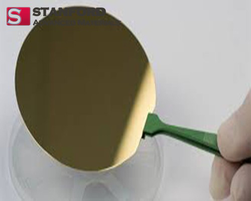
Stanford Advanced Materials (SAM) produces silicon wafer any diameters of from 2’’ (50.8 mm) to 12’’ (304.8mm) in order to provide the most flexibility as possible. With the aim of providing the largest range of specifications, we work either Cz (Czochralski) or FZ (Float Zone) silicon wafers.
Silicon wafer is a material used for producing semiconductors, which can be found in all types of electronic devices that improve the lives of people. It is the most common material and is widely used for a variety of high-tech industries. Due to the uniqueness of the electrical currents via silicon wafers, these semiconductors are used in creating ICs (integrated circuits) to act as commands for specific actions in various electronic devices.
|
Growth |
CZ / FZ |
|
Diameter |
Ø 2″ / Ø 3″ / Ø 4″ / Ø 6″ / Ø 8″ / Ø 12″ |
|
Thickness |
275 um ~ 775 um |
|
Orientation |
<100> / <111> / <110> or others |
|
SIIConductivity |
P – type / N – type / intrinsic |
|
Dopant |
Boron / Phosphorous / Antimony / Arsenic |
|
Resistivity |
0.001 ~ 10000 ohm-cm |
|
Surface |
One side polished / two sides polished |
|
TTV |
<= 10 um |
|
Bow / Warp |
<= 40 um |
|
Grade |
Prime / Test / Dummy grade |
|
CZ or FZ Wafer |
Prime Wafer |
|
Intrinsic Wafer |
Test Wafer |
|
Heavily Doped Wafer |
High Resistivity Wafer |
|
Off Axis Orientation Wafer |
Special Orientation Wafer |
|
Ultra Flat Wafer |
Ultra-Thin Wafer |
|
Ultra Thick Wafer |
Double Sides Polished |
|
Thermal Oxide Wafer |
Epi Wafer |
Silicon wafers have the following uses:
– Discrete
– Power device
– PW transistor IGBT
– MOS IC
– MEMS
– Solar cells
Further Reading:
P-type & N-type Silicon Semiconductors
Gallium Arsenide Wafer VS. Silicon Wafer
Submit your review | |