Electron Beam Evaporation VS Thermal Evaporation
Introduction
Electron beam evaporation and thermal evaporation are types of physical vapor deposition methods. Both processes have some similarities as well as differences. Ever wondered which of these processes is best for coating a substrate you’re working on? Read on.
What is Physical Vapor Deposition?
Physical vapor deposition is a method of coating substrates below atmospheric pressure. It is a type of vacuum deposition method. Some of the substrate materials coated using this method include ceramics, metals, and glass.
Physical vapor deposition methods pose fewer environmental threats than most other methods of thin-film deposition. In addition, physical vapor deposition methods produce coatings that are durable and resistant to corrosion. This process is commonly used for cutting tools, decoration, and anisotropic gasses
Electron Beam Evaporation
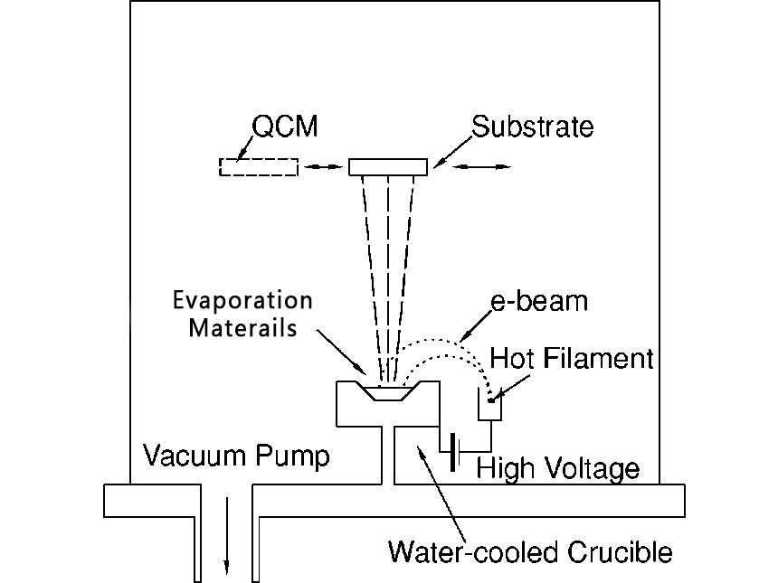
E-Beam evaporation is a type of physical vapor deposition. In this process, an electron beam from a charged tungsten filament bombards an anode target. This causes the atoms from the target to transition into the gaseous state. Subsequently, the gaseous atoms precipitate into the solid phase, coating the contents of the vacuum chamber. In this process, coating occurs exclusively within the line of sight.
Advantages
- Electron beam vapor deposition heats materials to higher temperatures than most other methods of PVD. Hence, this physical vapor deposition method has a high deposition rate.
- It produces thinner films than thermal evaporation.
- Electron beam evaporation gives rise to products of high purity.
- The coating is more easily controlled with electron beam evaporation.
- It is ideal for metals with a high melting point.
- Film quality has a higher density than in the thermal evaporation method.
Disadvantages
- This method can not coat complex geometries completely. This is because it is a line-of-sight deposition process.
- When the tungsten filament degrades, the evaporation rate becomes non-uniform.
- It is more expensive than the thermal evaporation method.
Thermal Evaporation
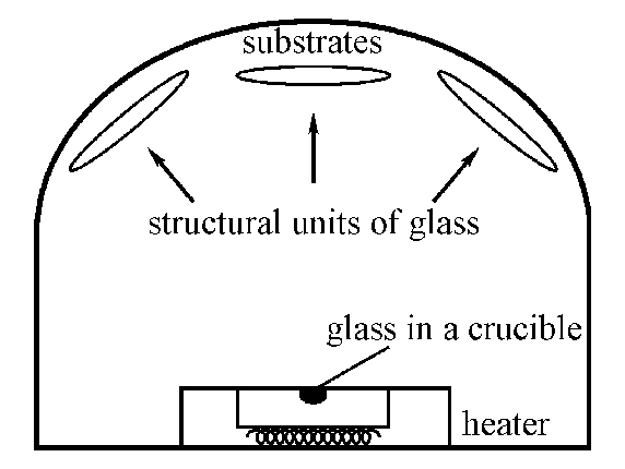
Thermal evaporation is a common method of physical vapor deposition. The deposited material in this method can be an atomic element or a molecule. Also, the substrate for this process can be semiconductors, solar cells, or optical components.
This process involves heating a solid material in a vacuum chamber. The material is heated in the vacuum chamber until it turns to vapor. The vapor stream from the material is then deposited on the substrate and adheres to it, forming a thin film or coating.
Siljegovi, M & Luki-Petrovi, S & Đačanin, Ljubica & Strbac, Dragana. (2022). Calculation of Single-layer and Multilayer Chalcogenide Refractive Index using Cheremukhins Method.
Advantages
- It can be easily used for both metals and nonmetals.
- It is ideal for materials that have a low melting point. These materials include alloys containing mercury.
- This physical vapor deposition process is easy to understand and implement,
- It is more affordable than most other methods of physical vapor deposition.
Disadvantages
- Its products have less purity than products from the electron beam evaporation method.
- Film quality is relatively low density.
Similarities & Differences
The major similarity between electron beam evaporation and thermal evaporation is that the two processes are physical vapor deposition processes. In both methods, the precursor material is converted to a vaporized state before depositing on the substrate.
The major difference between these two PVD evaporation methods lies in how they decompose a material before depositing it on the substrate. Interestingly, the name of these two processes can give you a peek into the difference between them. In electron beam evaporation, as the name implies, an electron beam evaporates the material. In this process, the material is not melted in the crucible. This is one of the reasons products from this process have high purity. However, in thermal evaporation, the material is heated in the crucible using electric resistance before it can be deposited on the substrate. This is one of the reasons that products from this process are impure. The challenge of impurity posited by this method can be overcome if a crucible is used to evaporate only one type of material.
Applications
Solar Cells
Both electron beam evaporation and thermal evaporation are used to coat thin-film solar cells. The materials used for this process include silicon, indium, CIGS, and etc.
OLEDS
Both processes are used to deposit the organic thin layers in the manufacture of OLEDs.
Optical Coating
These days, thin layers of materials are deposited on objects such as lenses and mirrors. These coatings can either decrease or increase reflections, depending on the purpose of the substrate.
Conclusion
When deciding which method to use between the electron beam evaporation method and the thermal evaporation method, one must put some factors into consideration. One must consider cost, durability, purity, yield, and quality. The points raised in this article help to make the decision a lot easier.


