(949) 407-8904 Mon - Fri 08:00 - 17:00 1940 East Deere Avenue, Suite 100, Santa Ana, CA 92705, USA

ST11214 Tantalum (Ta) Planar Sputtering Target

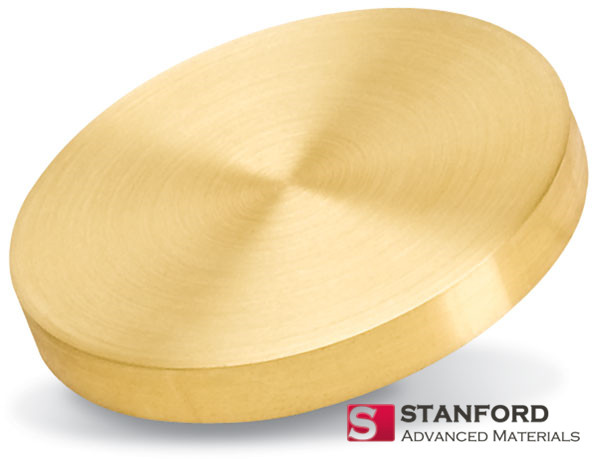
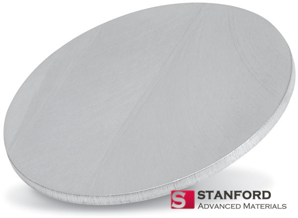
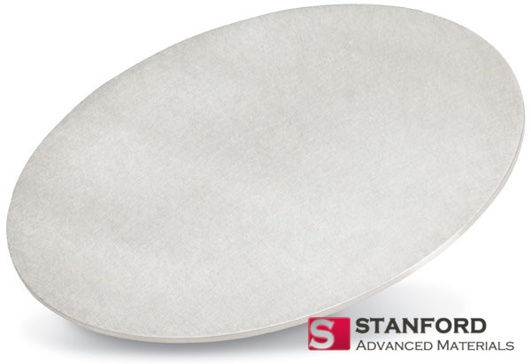
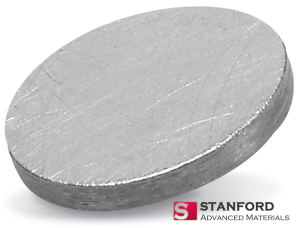
Our Tantalum (Ta) Planar Sputtering Targets are the benchmark for depositing ultra-stable, corrosion-resistant thin films. Essential for semiconductor and high-performance coating applications, tantalum provides unmatched thermal stability and chemical inertness in demanding environments.

Material Tantalum (Ta)
Purity ≥ 99.95% (Metal Basis)
Form Planar Sputtering Target
Standard Shape Rectangular / Circular (Customizable)
Key Properties Melting Point: ~3017℃ | Density: ~16.6 g/cm³ | Excellent Corrosion Resistance

Key Advantage: Enables deposition of films with outstanding thermal stability and diffusion barrier performance. High purity and controlled microstructure ensure low particulate contamination and excellent film uniformity.

Customization: Purity (≥99.95% – 99.999%), dimensions (thickness, width, length, diameter), surface finish, and bonding (to Cu/Al backing plates) are fully customizable to your system requirements.

Typical Applications: Diffusion barrier/liner layers in semiconductor Cu interconnects; corrosion-resistant coatings for medical implants and chemical equipment; gate electrodes in advanced logic devices.


Description

Complete Technical Specifications & Capabilities

Comprehensive specifications for process integration and material selection. All parameters can be customized to fit specific system configurations and film requirements.

Parameter Specification / Details
Material Tantalum (Ta)
Purity ≥ 99.95% (Standard), ≥ 99.99% and higher grades available upon request.
Crystal Structure Body-Centered Cubic (BCC) – α-Ta phase (desirable for low resistivity films).
Density ~16.6 g/cm³ (Theoretical)
Melting Point Approx. 3017 °C (5453 °F)
Thermal Conductivity ~57 W/(m·K) at 20°C
Electrical Resistivity ~13.5 nΩ·m at 20°C (For high-purity α-Ta)
Standard Shape Planar – Rectangular, Circular (Disc), or Custom Polygon
Dimensions Fully Customizable (Thickness, Length, Width, Diameter). Compatible with all major PVD system manufacturers.
Surface Finish Optimized for sputtering (e.g., fine-ground or polished) to minimize arcing and particulate generation.
Bonding Option Available bonded to copper, aluminum, or other backing plates using Inium, Elastomer, or high-temperature solders for efficient heat transfer.
Quality Documentation Certificate of Analysis (CoA) provided, including purity verification and lot traceability.

Technical & Application Deep Dive

1. The Semiconductor Workhorse: Ta as a Diffusion Barrier/Liner

Tantalum is indispensable in advanced semiconductor manufacturing, primarily for its role in copper interconnects:

  • Barrier Against Cu Diffusion: Ta films deposited from these targets form an excellent barrier that prevents copper from diffusing into the surrounding silicon dioxide or low-κ dielectric materials, which would cause device failure.
  • Promoting Adhesion & Microstructure: A thin Ta layer promotes the adhesion of subsequent copper seed layers and can influence the grain structure of the electroplated Cu fill, enhancing electromigration resistance.
  • Phase Matters (α-Ta vs. β-Ta): The low-resistivity, stable α-Ta phase is typically desired. Our manufacturing process is controlled to favor the formation of this phase in the target, promoting its deposition in the film.

2. Beyond Semiconductors: Leveraging Tantalum’s Inherent Properties

The unique combination of properties makes Ta films suitable for diverse high-performance applications:

  • Biocompatible & Corrosion-Resistant Coatings: Tantalum oxide (Ta2O5) films, easily formed by reactive sputtering, are highly biocompatible and corrosion-resistant, making them ideal for medical implants (e.g., stents, orthopedic devices) and components exposed to harsh chemicals.
  • Protective Coatings for Optics & Tools: Ta and its nitride/oxide films provide durable, wear-resistant, and thermally stable coatings for precision optical components, cutting tools, and aerospace parts.
  • Fundamental Research: Used in studies on superconductivity (Ta is a Type-I superconductor below 4.47K), thin-film resistors, and as a substrate or electrode material in novel device architectures.

3. Advantages of the Planar Target Design for High-Purity Metals

The planar configuration is ideal for precision deposition processes using materials like tantalum:

  • Precision Film Thickness Control: Planar targets allow for highly controlled, uniform deposition over specific areas, which is critical for semiconductor wafer processing and precision optical coatings.
  • Compatibility with Complex System Geometries: Easily integrated into multi-target carousels for sequential or co-sputtering of different materials (e.g., TaN, TaSix).
  • Optimized for High-Power and Reactive Sputtering: Robust bonding options and the material’s own high melting point enable stable operation at high power densities, necessary for efficient deposition of dense Ta films or during reactive sputtering to form TaN or TaOx.

Quality Assurance & Manufacturing

Stanford Advanced Materials ensures the highest quality through stringent process controls:

  • Purity Verification: Final purity is confirmed using advanced analytical techniques like Glow Discharge Mass Spectrometry (GDMS) to detect trace impurities at the ppb level.
  • Microstructural Control: Grain size and orientation are carefully controlled through optimized melting (e.g., electron beam melting) and rolling/forging processes to ensure uniform erosion and consistent film properties.
  • Defect Minimization: Precision machining and ultrasonic cleaning are employed to achieve superior surface finish and eliminate particulate contamination.
  • Non-Destructive Testing (NDT): Ultrasonic inspection is used to check for internal bonding integrity and bulk material defects.

Why Choose SAM for Your Tantalum Targets?

  • Mastery of Refractory Metals: We possess deep expertise in processing high-melting-point, challenging metals like Tantalum to exacting specifications.
  • Focus on Semiconductor-Grade Quality: Our processes and controls are designed to meet the stringent contamination and uniformity requirements of the microelectronics industry.
  • Flexible Customization: We provide complete flexibility in dimensions, purity, bonding, and surface finish to match your specific cathode assembly and process recipe.
  • Global Supply Chain Reliability: Consistent quality and reliable delivery to support both R&D prototyping and high-volume manufacturing.

Next Steps: Get a Custom Quote

To receive a formal quotation or technical consultation, please provide:

  1. Required purity level (e.g., 99.95%, 99.99%).
  2. Target dimensions (Thickness x Width x Length or Diameter x Thickness) and desired shape.
  3. Bonding requirements (e.g., backing plate material and bonding type).
  4. Primary application (e.g., semiconductor barrier layer, medical coating, research) to guide optimal specification.
Request a Quote