(949) 407-8904 Mon - Fri 08:00 - 17:00 1940 East Deere Avenue, Suite 100, Santa Ana, CA 92705, USA

ST11209 CVD-Grade Silicon (Si) Sputtering Target

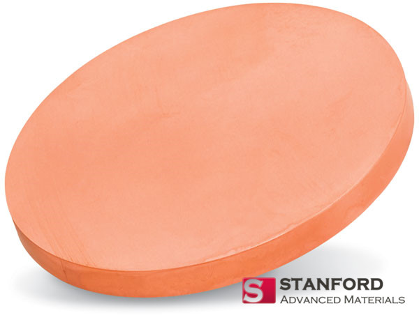
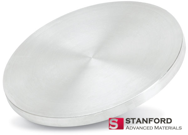
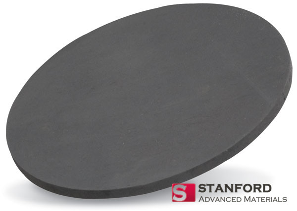
Our High-Definition Silicon (Si) Sputtering Target is engineered for applications demanding exceptional film uniformity and minimal particulates, such as advanced semiconductor front-end layers, high-efficiency thin-film photovoltaics, and precision optical coatings. The use of refined source materials and stringent process control ensures a target with superior density and a defect-minimized surface.

Material Silicon (Si)
Purity ≥ 99.99% (4N) Standard
Key Feature High Density & Low Surface Defect Count
Form Sputtering Target (Round or Rectangular)

Key Advantage: Controlled manufacturing minimizes micro-pores and inclusions, leading to stable, low-arcing sputtering performance and exceptionally smooth thin films.

Customization: Available in standard round or rectangular shapes. Purity (up to 99.999%), exact dimensions, and bonding to backing plates are fully customizable.

Typical Applications: Deposition of intrinsic/doped Si layers for semiconductors, absorber layers for a-Si/µc-Si solar cells, and Si-based films for IR optics and barrier coatings.

SKU: ST11209 Category: Tag:


Description

Complete Technical Specifications

For detailed evaluation and procurement (Product Code: ST11209).

Parameter Specification / Typical Value
Material Silicon (Si)
Purity (Standard) ≥ 99.99% (4N)
Production Method Refined Metallurgy / CVD-Grade Processes
Density ≥ 2.32 g/cm³
Key Impurity Control Low B, P, C, O content
Thermal Conductivity ~150 W/(m·K)
Available Shapes Round (Disc), Rectangular Planar
Dimensions Fully Customizable (Dia., Length, Width, Thickness)
Sputtering Method DC (for doped Si) or RF Magnetron Sputtering
Bonding Options Indium, Elastomer, or Specialty Solders
Surface Finish Fine-grained, defect-inspected (SEM analysis available)
Certification CoA with GDMS/Spark-OES impurity data and density report

Technical & Application Notes

1. Precision Source for Semiconductor Thin Films

This high-density, low-defect Si target is optimized for depositing critical layers where film homogeneity is paramount:

  • Gate & Local Interconnect Layers: Provides a uniform source for sputtered silicon films that may be subsequently doped, silicided, or patterned in advanced logic and memory devices.
  • Epitaxial-like or Polycrystalline Seed Layers: High-purity, dense films serve as high-quality seed layers for further epitaxial growth or as active poly-Si layers in devices.
  • Reactive Sputtering for Dielectrics: A clean, consistent Si target is ideal for reactive sputtering in N₂ or O₂ to form uniform silicon nitride (SiNₓ) or silicon oxide (SiOₓ) barrier or insulating layers.

2. Enabling High-Performance Photovoltaic & Optical Coatings

  • Thin-Film Solar Cell Absorbers: The low impurity and defect count contribute to superior electronic quality in amorphous (a-Si) or microcrystalline (µc-Si) absorber layers, directly impacting photovoltaic conversion efficiency and stability.
  • Infrared Optical Components: Silicon’s transparency in the IR range makes it valuable for anti-reflection and protective coatings on lenses and windows. A dense target yields films with optimal refractive index and low optical loss.

3. Critical for Advanced Research & Development

  • Multi-Layer Stack Deposition: The dimensional accuracy and surface flatness ensure reliable performance in complex multi-target deposition systems for research on superlattices or graded-composition films (e.g., SiGe).
  • Fundamental Thin-Film Studies: The well-characterized, high-quality target serves as a reliable reference material for studies on sputtering dynamics, film growth mechanisms, and structure-property relationships.

4. Process Stability & Target Longevity

The manufacturing focus on high density and defect control directly benefits the end-user process:

  • Reduced Arcing: Fewer micro-pores and inclusions minimize the risk of electrical arcing during sputtering, leading to higher process uptime and fewer film defects.
  • Uniform Erosion: A homogeneous microstructure promotes even target erosion, extending usable target life and maintaining consistent deposition rates over time.
  • Thermal Management: High density and good bonding ensure efficient heat transfer to the cooling plate, allowing for stable operation at optimal power levels.

Quality Assurance

We employ a multi-step inspection protocol to ensure target integrity:

  1. Density Verification: Precise measurement to ensure values meet or exceed theoretical density, minimizing porosity.
  2. Surface Defect Inspection: In-house electron microscopy (SEM) is used to identify and quantify surface imperfections, ensuring a sputter-ready finish.
  3. Compositional Certification: Trace element analysis via GDMS or Spark-OES provides detailed data on dopants and metallic impurities critical for electrical applications.

Why Stanford Advanced Materials (SAM) for This Grade

  • Focus on Microstructural Quality: We go beyond purity to guarantee high density and low defect counts for process stability.
  • Application-Specific Manufacturing: Processes are tailored based on whether the target is intended for electronic, photovoltaic, or optical applications.
  • Comprehensive Data Package: We provide not just a CoA, but also supporting data on density and surface quality upon request.

Request More Information

Discuss Your Precision Deposition Needs
To ensure the ST11209 grade meets your requirements, please specify:

  1. Primary application and required film properties (e.g., resistivity, optical transmission).
  2. Preferred shape (round/rectangular) and exact dimensions.
  3. Any specific concerns regarding process stability (e.g., arcing) or film defects.
Request a Quote