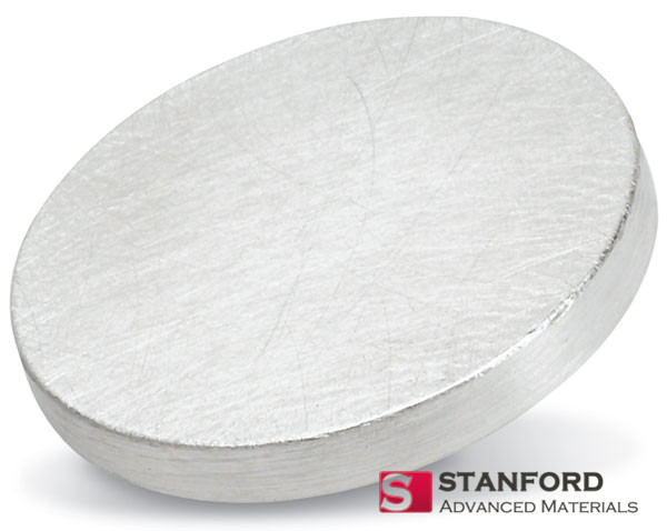
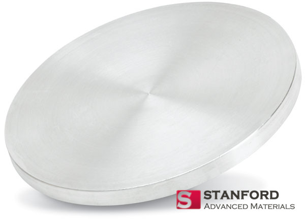
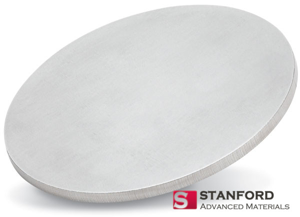
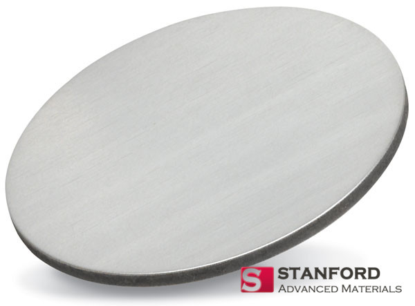
Our Niobium Planar Sputtering Targets are manufactured from the highest purity niobium metal, making them the material of choice for two of the most demanding thin-film applications: superconducting quantum devices and advanced semiconductor diffusion barriers. Where extreme purity dictates performance limits, our targets deliver.
| Material | Niobium (Nb) |
| Purity | ≥ 99.95% (3N5) Standard |
| Critical Property | High Superconducting Transition Temperature (Tc = 9.2 K) |
| Form | Planar Sputtering Target |
Key Advantage: Exceptionally low interstitial impurity levels (O, N, C, H) and metallic impurities (Ta, Fe) are critical for maximizing the superconducting performance and film quality in quantum and electronic applications.
Customization: Purity (up to 99.99%+ RRR grade), dimensions (thickness, length, width), and bonding fully customizable.
Typical Applications: Thin films for superconducting RF (SRF) cavities & qubits, Josephson junctions, diffusion barrier/liner layers in semiconductors, and corrosion-resistant coatings.
For detailed evaluation and procurement (Standard Reference: ST11197).
| Parameter | Specification / Typical Value |
|---|---|
| Material | Niobium (Nb) |
| Purity (Standard) | ≥ 99.95% |
| Available Purity (RRR) | 99.95%, 99.99% (RRR >300 available upon request) |
| Density | ≥ 8.57 g/cm³ |
| Crystal Structure | Body-Centered Cubic (BCC) |
| Superconducting Tc | 9.25 K (Bulk, High-Purity) |
| Melting Point | 2477 °C |
| Thermal Conductivity | 54 W/(m·K) |
| Standard Shape | Rectangular |
| Dimensions | Fully Customizable |
| Sputtering Method | DC Magnetron (Primary), HiPIMS |
| Bonding Options | Bonding to Cu backing plate recommended for high-power sputtering |
| Certification | Certificate of Analysis (CoA) with GDMS impurity data provided |
1. The Heart of Superconducting Quantum Devices
Niobium is the workhorse material for superconducting quantum computing and particle accelerator cavities. The performance of these devices is exquisitely sensitive to film purity and microstructure:
Superconducting Qubits: Thin Nb films are used in transmon and other qubit architectures. Impurities and defects create parasitic two-level systems (TLS), a major source of quantum decoherence. Our high-purity, fine-grained targets help minimize these losses.
SRF Cavities: Sputtered Nb films on copper cavities can offer performance and cost advantages over bulk Nb. High purity and density are essential to achieve high quality factors (Q) and accelerating gradients.
2. A High-Performance Barrier/Liner for Semiconductor Nodes
In semiconductor backend-of-line (BEOL) processing, niobium (and its nitride, NbN) is investigated as a diffusion barrier and liner for copper interconnects. Its high melting point, good adhesion, and ability to form a stable nitride make it a candidate for advanced nodes where traditional Ta/TaN barriers are scaled to their limits.
3. Why Purity and Microstructure are Non-Negotiable
Interstitial Control: Oxygen, nitrogen, and carbon interstitials can drastically suppress the superconducting Tc and increase residual resistivity. Our processing minimizes these.
Grain Structure: A fine, uniform grain structure in the target translates to a smooth, low-defect film, which is critical for both superconducting surface resistance and barrier layer continuity.
Metallic Impurities: Elements like tantalum (a common companion in ore) are rigorously controlled via multiple electron-beam melting passes.
For niobium targets destined for quantum applications, standard chemical analysis is insufficient. We provide Glow Discharge Mass Spectrometry (GDMS) data, quantifying critical impurities at the parts-per-million (ppm) and even parts-per-billion (ppb) level. Residual Resistivity Ratio (RRR) measurements can be performed on sample material to directly indicate electronic purity. This level of documentation is essential for your research or production qualification.
Quantum & SRF Materials Specialist: We supply materials to leading national labs, universities, and companies in the quantum and accelerator sectors.
Ultra-High Purity Focus: We specialize in metals where trace impurities define functional performance, not just chemical composition.
From Research to Pilot Production: We support both small-scale R&D projects and the scaling needs of emerging quantum hardware manufacturers.
Get a Formal Quote or High-Sensitivity CoA
For applications where purity is critical, please provide:
Required purity grade and any specific impurity limits (e.g., max O, Ta content).
Target dimensions and intended sputtering system.
Primary application (e.g., qubit film deposition, SRF cavity coating, semiconductor barrier research).