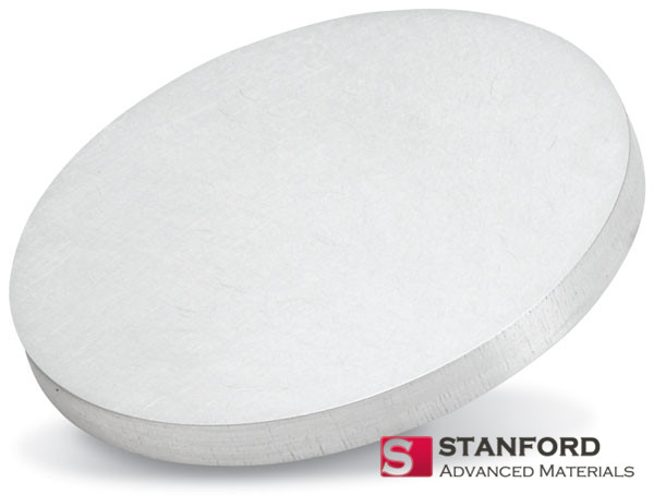
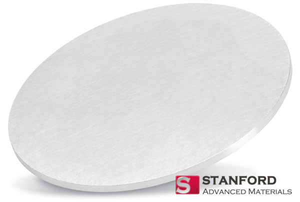
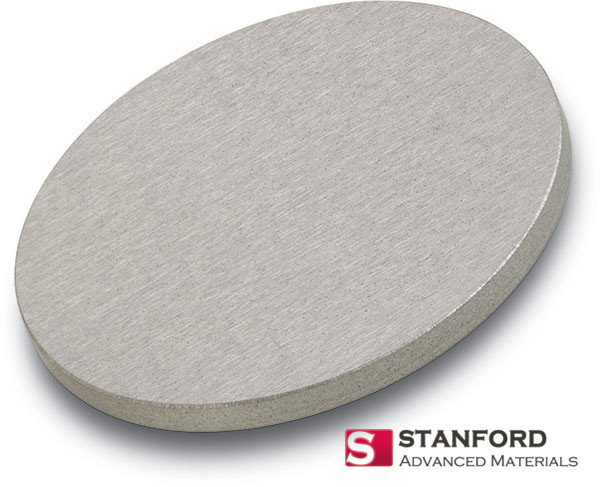
Our Aluminum Silicon (AlSi) alloy sputtering targets are engineered to overcome the limitations of pure aluminum, offering improved electromigration resistance, finer microstructure, and better thermal stability for advanced semiconductor metallization and high-efficiency solar cell applications.
| Material | Aluminum Silicon Alloy (AlSi) |
| Typical Si Content | 0.5% – 12% (Customizable) |
| Purity | ≥ 99.99% (Metal Basis) |
| Form | Planar Sputtering Target |
Key Advantage: Silicon addition suppresses aluminum grain growth and hillock formation, significantly improving film reliability and enabling finer line geometries.
Customization: Silicon content, dimensions (thickness, length, width), and bonding fully tailored to your process.
Typical Applications: Semiconductor interconnects (especially for ≤ 0.18µm nodes), silicon solar cell front/back contacts, diffusion barrier layers, and microelectronics.
For detailed evaluation and procurement (Standard Reference: ST11170).
| Parameter | Specification / Capability | Notes / Process Relevance |
|---|---|---|
| Material | Aluminum-Silicon (AlSi) Alloy | — |
| Silicon Content | 0.5% to 12% by weight (Standard: 1%) | Critical parameter. Lower Si (~0.5-1%) for interconnects; higher Si (up to 12%) for contacts/barriers. |
| Base Purity | ≥ 99.99% (4N) on Metal Basis | High purity of Al and Si minimizes impurities that affect film resistivity and junction leakage. |
| Density | ≥ 2.70 g/cm³ (Varies with Si%) | Near-theoretical density ensures uniform thermal/electrical properties and stable sputtering. |
| Microstructure | Fine, Homogeneous Si distribution in Al matrix | Prevents Si nodule formation and ensures uniform film composition and resistivity. |
| Standard Shape | Rectangular | Circular and other custom geometries available. |
| Dimensions | Fully Customizable (Thickness ≥ 1mm) | Sized for your PVD chamber and throughput requirements. |
| Electrical Resistivity | Slightly higher than pure Al, varies with Si% (e.g., Al-1%Si: ~3.0 µΩ·cm) | A known, controllable trade-off for vastly improved reliability. |
| Thermal Conductivity | ~200-220 W/(m·K) (Varies with Si%) | Remains highly effective for heat dissipation during sputtering. |
| Sputtering Method | DC Magnetron (Primary) | Standard for conductive alloy targets. |
| Bonding Options | Indium, Epoxy, or specialty solder to Cu/SS backing plate | Ensures mechanical stability and efficient cooling. |
| Certification | Certificate of Composition (CoC) provided | Verifies exact Si content and overall purity via ICP-OES or similar analysis. |
1. Silicon’s Role: From Problem Solver to Enabler
In semiconductor manufacturing, pure aluminum interconnects suffer from electromigration (mass transport under high current density) and hillock formation (protrusions during thermal cycling). The addition of even small amounts of silicon (traditionally 0.5-1%) effectively pins grain boundaries, dramatically reducing these failure mechanisms and enabling reliable operation at smaller technology nodes.
2. Composition Precision & Microstructural Control
The key to an effective AlSi target is not just the average silicon content, but its uniform distribution. We employ rapid solidification techniques or specialized powder metallurgy to achieve a fine, supersaturated solid solution or a fine dispersion of Si particles. This prevents localized “Si nodules” that can cause arcing during sputtering or create defects in the deposited film.
3. Application-Specific Guidance
Each AlSi target batch is validated for composition using Inductively Coupled Plasma Optical Emission Spectroscopy (ICP-OES). Microstructural homogeneity is verified via Scanning Electron Microscopy (SEM) with Energy Dispersive X-ray (EDX) mapping to confirm the uniform distribution of silicon. This ensures predictable and repeatable sputtering performance.
Get a Formal Quote or Composition Datasheet
To specify the optimal target for your process, please provide: