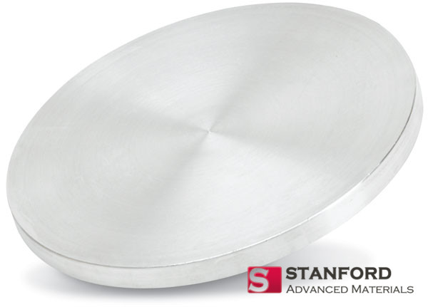
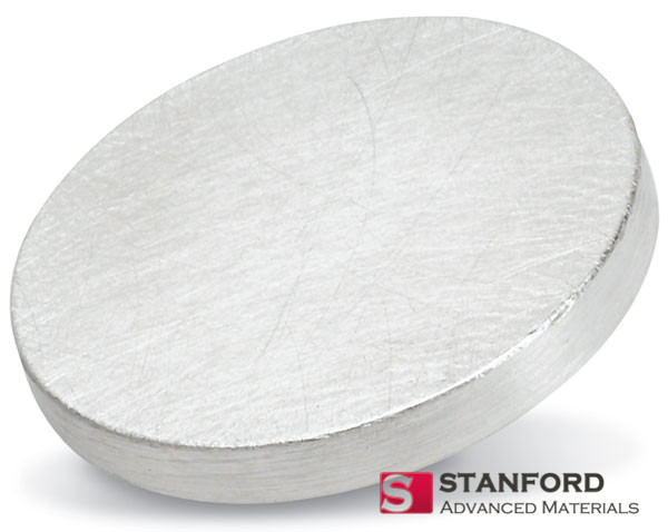
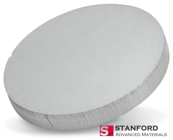
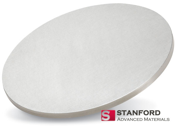
Engineered for superior process stability, our high-purity Aluminum Planar Targets deliver consistent film uniformity and excellent step coverage, making them the industry standard for conductive and reflective layers in demanding semiconductor and optical applications.
| Material | Aluminum (Al) |
| Purity | ≥ 99.99% (4N) |
| Form | Planar Sputtering Target |
| Shape | Rectangular (Standard) |
Key Advantage: Ultra-high purity and controlled grain structure for low-defect, uniform deposition with excellent adhesion and conductivity.
Customization: Thickness, length, width, and bonding options fully customizable to your sputtering system.
Typical Applications: Semiconductor interconnects & metallization, photovoltaic back contacts, optical reflectors, and barrier/seed layers.
For detailed evaluation and procurement (Standard Reference: ST11166).
| Parameter | Specification / Typical Value | Notes / Process Relevance |
|---|---|---|
| Material | Aluminum (Al) | — |
| Purity (Standard) | ≥ 99.99% (4N) | Minimizes impurities (e.g., Si, Fe, Cu) that affect film resistivity, reflectivity, and corrosion resistance. |
| Density | ≥ 2.69 g/cm³ (Theoretical: 2.70 g/cm³) | High density ensures stable thermal management and consistent sputter yield. |
| Grain Structure | Fine, Equiaxed | Controlled to reduce particle generation and ensure uniform erosion across the target face. |
| Standard Shape | Rectangular | Circular and other custom geometries available upon request. |
| Minimum Thickness | ≥ 1 mm | Custom thicknesses available to optimize target life for your power/throughput requirements. |
| Thermal Conductivity | ~235 W/(m·K) | Excellent for heat dissipation, enabling stable operation at higher power densities. |
| Electrical Resistivity | ~2.65 µΩ·cm @ 20°C | Baseline property for high-conductivity aluminum films. |
| Melting Point | 660.3 °C | — |
| Coeff. of Thermal Expansion | ~23.1 x 10⁻⁶ /K | Critical parameter for bonding compatibility and thermal cycle stability. |
| Sputtering Method | DC Magnetron (Primary), RF compatible | Optimized for high-rate DC deposition. |
| Bonding Options | Indium, Elastomer, or specialty solder to Cu/SS backing plate | Ensures optimal thermal contact and prevents debonding during operation. |
| Certification | Certificate of Analysis (CoA) provided | Confirms purity and key physical properties. |
1. The Critical Role of Purity in Performance
Our ≥99.99% purity specification is engineered to minimize key impurities that degrade film performance. For example, controlling silicon and iron content is crucial for achieving low film resistivity in semiconductor interconnects, while managing copper and other transition metals enhances long-term corrosion stability in optical and reflective coatings.
2. Engineered for Process Stability & High Yield
Aluminum’s combination of good thermal conductivity and a relatively low melting point necessitates precise control over target microstructure. Our targets are processed to achieve a fine, uniform grain structure, which is essential for minimizing arcing—a common source of film-defect-causing macro-particles—especially in high-power DC sputtering processes.
3. Application-Specific Guidance
Every Aluminum Planar Target is subject to rigorous multi-point inspection, including surface roughness measurement, dimensional verification via CMM or laser scanning, and microstructural analysis (SEM/EDS) to confirm grain size and homogeneity. Final cleaning and packaging are performed in a controlled environment to prevent oxidation and contamination.
Get a Formal Quote or Technical Datasheet
To obtain a precise quotation and specifications tailored to your needs, please provide: