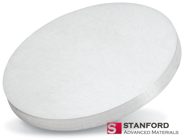
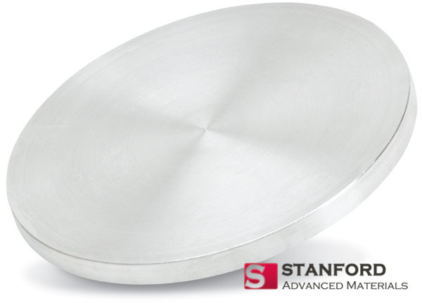
| Chemical Formula | Ge-As-Se |
| Catalog No. | ST0984 |
| CAS Number | 57673-50-4 |
| Purity | 99.9%, 99.95%, 99.99%, 99.995%, 99.999% |
| Shape | Discs, Plates, Column Targets, Step Targets, Custom-made |
With a strong commitment to superior quality and cost-effectiveness, Stanford Advanced Materials (SAM) specializes in providing Germanium Arsenide Selenide Sputtering Targets. SAM ensures clients unparalleled quality without compromising affordability, making these sputtering targets the preferred option in the market.
Germanium Arsenide Selenide Sputtering Targets boast a plethora of distinctive properties, rendering them highly sought-after in the realm of high-tech applications. Among their standout features is superior electrical conductivity, making them an ideal choice for the manufacturing of electronic devices. The targets exhibit excellent thermal stability, ensuring their resilience in the face of high temperatures and thermal stress, further solidifying their suitability for electronic device fabrication. Moreover, the Germanium Arsenide Selenide Sputtering Targets showcase exceptional chemical stability, enabling them to endure the intricacies of complex manufacturing environments without compromising performance.
Beyond their electronic applications, these targets shine in the field of optoelectronics and laser device manufacturing, owing to their special optical properties. This unique attribute allows Germanium Arsenide Selenide Sputtering Targets to fulfill a pivotal role, enhancing the precision and efficiency of devices in these cutting-edge technologies. In essence, the multifaceted nature of Germanium Arsenide Selenide Sputtering Targets positions them as an indispensable material, laying a robust foundation for advancements in diverse high-tech domains
Related Product: Copper Gallium Selenide Sputtering Target, Bismuth Antimony Selenide Sputtering Target
| Compound Formula | Ge-As-Se |
| Appearance | Gray Target |
| Melting Point | >360℃ |
| Density | 4.4-4.62 g/cm3 |
| Available Sizes | Dia.: 1.0″, 2.0″, 3.0″, 4.0″, 5.0″, 6.0″
Thick: 0.125″, 0.250″ |
Germanium Arsenide Selenide Sputtering Targets are widely used in many fields, and their unique properties make them key materials in high-tech manufacturing. It plays an important role in electronic device manufacturing, using its superior electrical conductivity and thermal stability to produce high-performance semiconductor devices, including transistors and integrated circuits. In addition, Germanium Arsenide Selenide Sputtering Targets also show their talents in the field of optoelectronics. Their special optical properties make them ideal for manufacturing laser devices and photodetectors. Its application in optical communications and laser technology provides excellent performance support for information transmission and laser applications. Germanium Arsenide Selenide Sputtering Targets also play a role in the manufacture of solar cells, making full use of their electrical and optical properties to improve solar energy conversion efficiency.
Our Germanium Arsenide Selenide Sputtering Target is carefully handled during storage and transportation to preserve the quality of our products in their original condition.
SAM’s Germanium Arsenide Selenide Sputtering Target is available in various forms, purities, and sizes. We specialize in producing high-purity physical vapor deposition (PVD) materials with the highest possible density and smallest possible average grain sizes for use in semiconductor, chemical vapor deposition (CVD), and physical vapor deposition (PVD) display and optical applications.