What Are the Uses of Molybdenum Sputtering Targets?
Molybdenum sputtering targets can form films on various kinds of substrates, which are widely used as electronic components and products. In this article, we will explore the various applications of molybdenum sputtering targets. These targets play a vital role in the electronics and renewable energy industries, enabling the deposition of thin films on diverse substrates. Let’s delve into the main uses of molybdenum sputtering targets.
Properties of Molybdenum Sputtering Target
In the electronics industry, molybdenum sputtering targets find applications in flat panel displays, thin-film solar cell electrodes, wiring materials, and semiconductor barrier layers. Molybdenum’s high melting point, conductivity, low specific impedance, corrosion resistance, and environmental performance make it an ideal choice for these applications. Compared to chromium, molybdenum’s lower specific impedance and membrane stress, along with its lack of environmental pollution concerns, make it a preferred material for flat panel display sputter targets. Additionally, incorporating molybdenum components in LCD enhances its brightness, contrast, color, and overall lifespan.
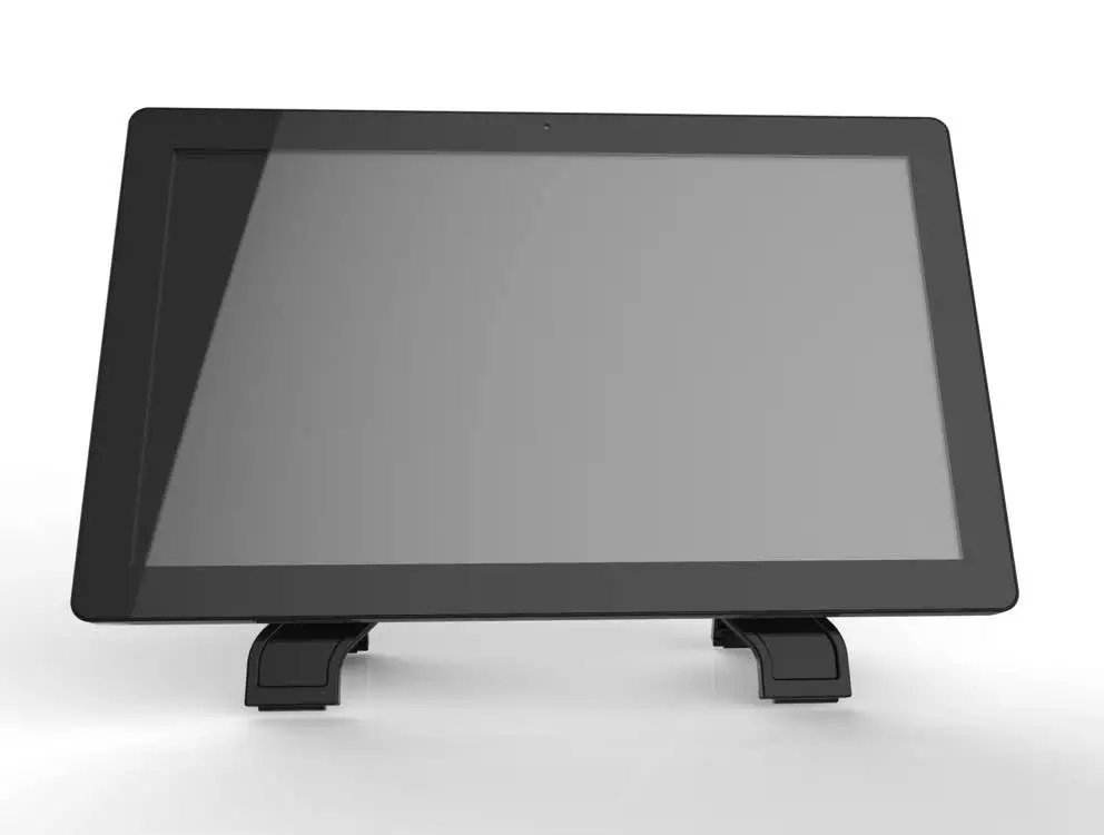
Uses of Molybdenum Sputtering Targets for Flat Panel Display
In the electronics industry, uses of molybdenum sputtering targets mainly inxlude planar displays, thin film solar cell electrode and wiring material and semiconductor barrier layer materials, which are based on molybdenum with the high melting point, high conductivity, low specific impedance, good corrosion resistance and good environmental performance. Molybdenum has the advantages of specific impedance and membrane stress only half that of chromium, and there is no environmental pollution problem, so it has become one of the preferred materials for sputter target of the flat panel display. Besides that, the use of molybdenum in the components of LCD can greatly improve the performance of LCD in brightness, contrast, color, and life.
One of the main markets driving the demand for molybdenum sputtering targets is TFT-LCD (Thin-Film Transistor Liquid Crystal Display) in the planar display industry. Market research indicates that the next few years will witness significant LCD development, with an estimated annual growth rate of about 30%. As the LCD market expands, the consumption of target materials, including molybdenum sputtering targets, is expected to rise rapidly, with an annual growth rate of approximately 20%.
Uses of Molybdenum Sputtering Targets for Thin-film Solar Photovoltaic Cells
Beyond planar displays, the usage of molybdenum sputtering targets is also increasing in thin-film solar photovoltaic cells, driven by the growing renewable energy industry.
Thin-film solar cells, particularly copper indium gallium selenide (CIGS) thin film solar cells, benefit from molybdenum sputtering targets. CIGS solar cells, comprising copper, indium, gallium, and selenium, demonstrate strong light absorption, high power generation stability, and high conversion efficiency. Molybdenum, forming the electrode layer of CIGS thin film batteries through splatter plating, plays a crucial role in nucleation, growth, and morphology of the CIGS thin film crystal.
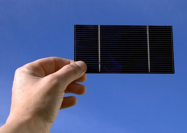
The target material of molybdenum mainly forms the electrode layer of the CIGS thin film battery by splatter plating. Molybdenum is at the bottom of the solar cell. As the back contact of the solar cell, it plays an important role in nucleation, growth, and morphology of CIGS thin film crystal.
Conclusion
The versatile applications of molybdenum sputtering targets are driving their demand in the electronics and renewable energy sectors. As a leading sputtering target manufacturer, Stanford Advanced Materials (SAM) is a leading sputtering target manufacturer based in Lake Forest, California. If you feel interested in the molybdenum sputtering targets, you can go to our product page for more information, or directly send us an inquiry. You can also contact us via target@samaterials.com. Free samples are available.


