Preparation of CIGS absorber layer
1. Preparation of Cu/In film by magnetron sputtering
In order to accurately control the element ratio of Cu/In, CuIn film is prepared by the co-sputtering method. That is, the Cu/In alloy target and the In elemental target are simultaneously sputtered in the same sputtering chamber. The distribution of Cu/In content has a great influence on the performance of the film. From the morphology analysis, when the Cu content is high, the film is a distinct mirror surface, which is characterized by metallic luster. When the In content is high, the surface is dark red. Due to the small grain size of the In-rich film, the selenization process can form CIS and CIGS films with good crystallization and smooth surface morphology. Therefore, the precursors used are all In-rich films.
2. Preparation of CuInGa film by magnetron sputtering
Replacing the In element with a certain amount of Ga in CuInSe2 can change the band gap of the alloy semiconductor film. As the Ga element increases, the band gap is adjustable from 1.04 eV to 1.68 eV. However, the addition of Ga tends to cause cracking of the film. The higher the Ga content is, the more obvious the cleaving phenomenon is. And a high concentration of Ga easily forms a Cu1-xSe heterophase on the surface of the film, affecting the open circuit voltage and electron transport of the battery. This phenomenon can be confirmed by XRD characterization. It is found that the solar cell performance is optimal when the ratio of Ga element substitution to In is controlled at about 30%.
3. Preparation of CIGS film by CVD (chemical vapor deposition)
In the experiment, the CuInGa film was usually subjected to a two-step selenization treatment using a CVD system to prepare a CIGS film. Because the gas H2Se is toxic and costly, solid-state selenium powder is often used in the laboratory to substitute for the traditional gas selenium source. The first step of selenization allows the solid selenium source to be fully vaporized to achieve a higher selenide vapor concentration, providing a basis for the second step of selenization. The second step of selenization is to thermally selenize the CIG alloy film to prepare the CIGS absorber layer. The effect of temperature on selenization is particularly obvious.
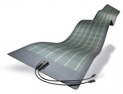
Stanford Advanced Materials (SAM) is a global sputtering targets manufacturer which supplies high-quality and consistent products to meet our customers’ R&D and production needs. e provide high purity CIGS materials and we ensure you will be satisfied with our products. Please visit our website https://www.sputtertargets.net/ for more information.
Further Reading: An Introduction to CIGS Thin-Film Photovoltaics


