| Catalog No. | IN2271 |
|---|---|
| Material | InAs |
| Thickness | 500 um- 625 um |
| Conductive Type | N – type/ P- type |
| Diameter | Ø 2″ Ø 3″ |
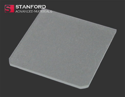
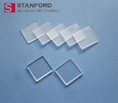
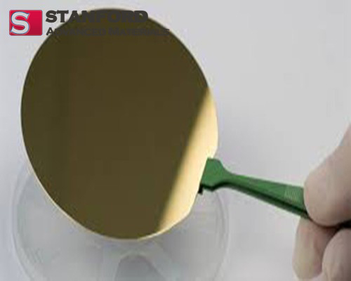
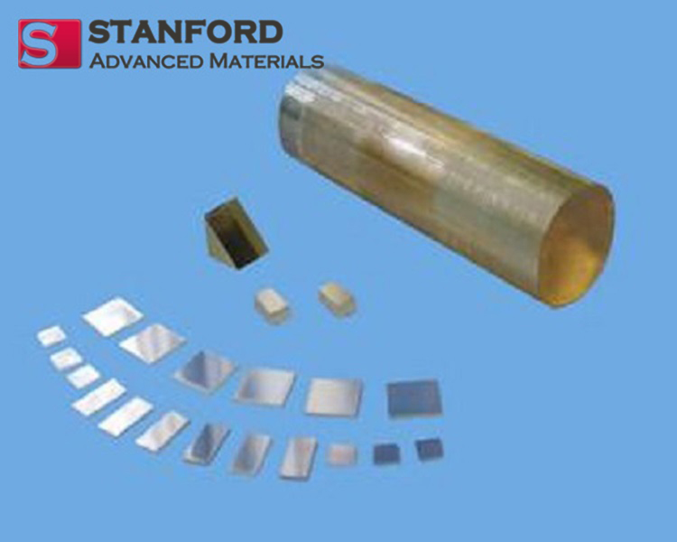
Stanford Advanced Materials (SAM) provides high quality single crystal indium arsenide wafer to the electronic and optoelectronic industry in diameter up to 3 inches.
Indium arsenide wafer is made of a crystalline compound made by 6N pure In and As element and is grown by Liquid Encapsulated Czochralski (LEC) method with EPD < 15000 cm -3. InAs crystal has high uniformity of electrical parameters and low defect density, suitable for MBE or MOCVD epitaxial growth. We have “epi ready” InAs products with a wide choice in exact or off orientation, low or high doped concentration and surface finish. Please contact us for more product information.
|
Growth |
LEC |
|
Diameter |
Ø 2″ / Ø 3″ |
|
Thickness |
500 um – 625 um |
|
Orientation |
<100> / <111> / <110> or others |
|
Off orientation |
Off 2° to 10° |
|
Surface |
One side polished or two sides polished |
|
Flat options |
EJ or SEMI. Std . |
|
TTV |
<= 10 um |
|
EPD |
<= 15000 cm-2 |
|
Grade |
Epi polished grade / mechanical grade |
|
Package |
Single wafer container |
Indium arsenide wafer has the following applications:
– Used in higher-power applications at room temperature
– Used for making of diode lasers
– Construction of infrared detectors
Submit your review | |