| Catalog No. | GA2269 |
|---|---|
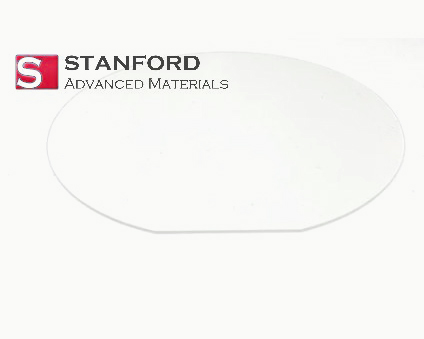
| Material | GaP |
| Thickness | 400um |
| Conductive Type | N – type |
| Diameter | Ø 2″ |
Stanford Advanced Materials (SAM) provides high quality single crystal GaP gallium phosphide wafer to the electronic and optoelectronic industry in diameter up to 2 inches.
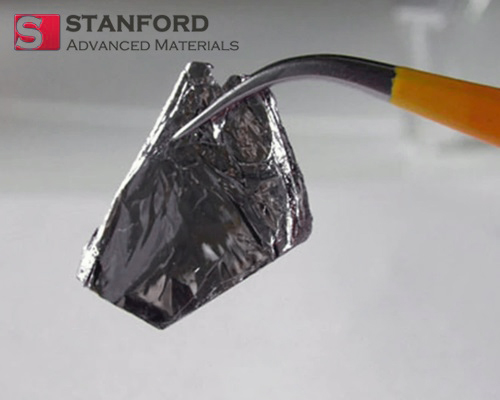
GaP single crystal is usually grown by LEC technique using 6N high purity materials. Gallium phosphide wafer is an important semiconductor material that has unique electrical properties as other III-V compound materials and is widely used as red, yellow, and green LED (light-emitting diodes).
| Growth | LEC |
| Diameter | Ø 2″ |
| Thickness | 400 um |
| Orientation | <100> / <111> / <110> or others |
| Off orientation | Off 2° to 10° |
| Surface | One side polished or two sides polished |
| Flat options | EJ or SEMI. Std . |
| TTV | <= 10 um |
| EPD | <= 2E5 cm-2 |
| Grade | Epi polished grade / mechanical grade |
Gallium phosphide wafer is used in Opto device: Visible LED such as display element (red, green) and backlight of LCD (yellow, green) etc.
Submit your review | |
The wafer arrive with the speed i had to blink. The quality is exactly what i was wishing for. They are really well-made.