Everything You Need to Know About Molybdenum Sputter Targets
Introduction to Molybdenum Sputter Targets
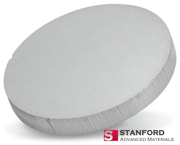
In the realm of material science and thin-film technology, molybdenum sputter targets hold a pivotal position. These targets, crafted from molybdenum, a transition metal known for its high melting point and remarkable thermal and electrical conductivity, are instrumental in the physical vapor deposition (PVD) process.
This process is critical for applying thin film coatings on various substrates, which find applications across a multitude of industries. This article delves into the manufacturing process, applications, benefits, and challenges of molybdenum sputtering targets, providing a comprehensive understanding of their significance in contemporary technology.
Manufacturing Process of Molybdenum Sputter Targets
The production of molybdenum sputter targets involves a series of sophisticated steps, each critical to ensuring the final product meets the stringent requirements for thin-film deposition applications.
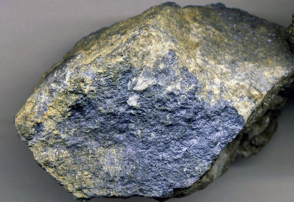
1. Extraction and Purification of Molybdenum Ore
The process starts with mining molybdenite ore, the primary source of molybdenum. The ore undergoes flotation to concentrate the molybdenite mineral, followed by a series of chemical reactions to purify the molybdenum. Roasting converts molybdenite to molybdenum oxide, which is then reduced to pure molybdenum metal through hydrogen reduction. This stage is crucial for removing impurities that could negatively impact the sputtering performance.
2. Powder Metallurgy
The pure molybdenum metal is then converted into fine powder. This powder metallurgy process involves atomization or mechanical milling, which breaks down the metal into a fine powder. The powder’s particle size and distribution are carefully controlled to ensure uniformity, a critical factor for achieving consistent density and mechanical properties in the final target.
3. Pressing and Sintering
The molybdenum powder is next pressed into a compact shape, often under high pressure, to form a green body. This body is then sintered at high temperatures in a protective atmosphere, causing the powder particles to bond together. Sintering not only densifies the material but also helps in achieving the desired purity and grain structure. The sintering conditions, including temperature and duration, are optimized to enhance the mechanical and physical properties of the ingot.
4. Rolling, Forging, and Machining
The sintered ingot undergoes rolling and forging processes to achieve the desired thickness and shape, improving its microstructure and mechanical properties. These mechanical deformation processes break up the grain structure, making it more uniform. The ingot is then machined to the precise dimensions required for sputter targets. This includes cutting to size, surface finishing, and sometimes drilling holes or adding features for mounting in sputtering systems. The machining process must be meticulously controlled to avoid introducing surface imperfections or stresses that could affect sputtering performance.
5. Quality Control and Inspection
Throughout each stage of the manufacturing process, rigorous quality control measures are implemented. This includes inspections for purity, density, grain size, and absence of defects. Advanced techniques such as X-ray diffraction (XRD), scanning electron microscopy (SEM), and energy-dispersive X-ray spectroscopy (EDX) may be employed to analyze the material’s structural and compositional properties. Ensuring the molybdenum sputter target meets the specific criteria is vital for achieving uniform thin films with excellent electrical, thermal, and mechanical properties.
Benefits of Molybdenum Sputter Targets
Molybdenum, with its unique set of properties, stands out as a sputtering target material for several reasons:
High Melting Point and Thermal Stability
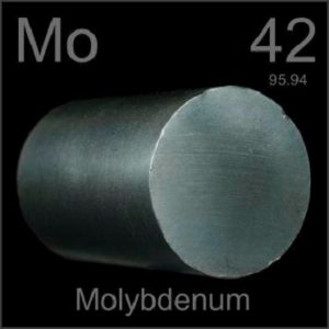
Molybdenum boasts a melting point of 2,623°C (4,753°F), which not only facilitates deposition processes at high temperatures but also ensures the structural integrity of the target under extreme conditions. This high melting point is instrumental in enabling high-temperature sputtering processes, which are often required to achieve optimal film adhesion and microstructural properties.
The thermal stability of molybdenum, characterized by its ability to retain its physical and chemical properties over a wide temperature range, plays a critical role in achieving uniform thin films with exceptional quality. This stability minimizes the risk of target degradation and contamination, leading to more reliable and consistent deposition outcomes.
Superior Electrical Conductivity
The electrical conductivity of molybdenum is another key benefit, especially in applications requiring the deposition of conductive layers. Molybdenum films can effectively serve as conductive pathways in electronic devices, offering low resistance and high efficiency. This property is crucial in the fabrication of integrated circuits, thin-film transistors, and other components where electrical performance is paramount. The efficient conductive layers provided by molybdenum sputtering targets contribute to the overall performance, energy efficiency, and miniaturization of electronic devices.
Consistent Sputtering Rates and Uniform Film Thickness
The density and uniform grain structure of molybdenum targets are essential for achieving consistent sputtering rates and uniform film thickness across the substrate. A uniform grain structure ensures that the sputtering process proceeds at a steady rate, minimizing variations in film thickness and composition. This uniformity is critical for applications requiring precise control over the film’s optical, electrical, and mechanical properties. For instance, in the manufacturing of semiconductors and photovoltaic cells, where even minor inconsistencies can significantly impact device performance, the consistency offered by molybdenum targets is invaluable.
Enhanced Performance and Longevity of Coated Devices and Components
The advantages mentioned above directly contribute to the enhanced performance and longevity of devices and components coated with films deposited using molybdenum sputter targets. The high-quality films improve the durability, efficiency, and reliability of the final products.
For example, in the context of solar panels, molybdenum-based back contacts can improve the electrical conductivity and corrosion resistance of the cells, leading to higher energy conversion efficiencies and longer operational lifetimes. Similarly, in the realm of display technologies, molybdenum layers can enhance the performance and durability of the components, ensuring that they withstand the rigors of everyday use without degradation.
Applications of Molybdenum Sputter Targets
Semiconductor Industry
In the semiconductor sector, molybdenum sputter targets are indispensable for creating thin films that serve as barriers, adhesion layers, or conductive paths in integrated circuits (ICs). Molybdenum’s high melting point and excellent electrical conductivity make it suitable for forming the metallization layers that connect different parts of a semiconductor device, ensuring reliable performance even under high power and temperature conditions.

Flat Panel Displays
The use of molybdenum targets in the flat panel display industry is crucial for producing thin-film transistors (TFTs) and electrodes in liquid crystal displays (LCDs), organic light-emitting diodes (OLEDs), and touchscreens. Molybdenum films contribute to the display’s functionality and durability, providing the electrical conductivity required for pixel activation while maintaining transparency and resistance to environmental degradation.
Photovoltaic Cells
In solar energy applications, molybdenum sputter targets are used to deposit back contact layers on thin-film photovoltaic cells, such as copper indium gallium selenide (CIGS) and cadmium telluride (CdTe) solar cells. These molybdenum layers are crucial for ensuring efficient electron flow and enhancing the cell’s overall energy conversion efficiency. The material’s stability under high temperatures and corrosion resistance contribute to the longevity and performance of solar panels.
Thin-Film Transistors
Molybdenum is pivotal in manufacturing thin-film transistors, a fundamental component of many electronic displays and circuits. Its films serve as the gate electrode, providing the necessary conductivity and stability for the effective control of current flow within the device. This application underscores molybdenum’s role in advancing display technologies and flexible electronics.
Aerospace
The aerospace industry leverages molybdenum coatings for their exceptional strength-to-weight ratio, high-temperature resistance, and corrosion resistance. Components such as turbine blades, engine nozzles, and heat shields benefit from molybdenum’s durability and performance in extreme conditions, contributing to the reliability and longevity of aerospace machinery and equipment.
Automotive Industry
In automotive applications, molybdenum sputter targets are used to deposit coatings on various parts, including electrical contacts, sensors, and protective layers on glass. These coatings enhance the components’ resistance to wear, corrosion, and high temperatures, improving vehicle performance and safety.
Medical Devices
The biocompatibility and corrosion resistance of molybdenum make it ideal for medical device applications, including implants and surgical instruments. Thin molybdenum coatings can provide a barrier against corrosion and wear, extending the lifespan of medical devices while ensuring safety and reliability in medical procedures.
Protective Coatings
Beyond its electrical and thermal applications, molybdenum is used in protective coatings for industrial machinery and tools. Its resistance to wear, corrosion, and high temperatures protects equipment in harsh industrial environments, enhancing durability and reducing maintenance costs.
Read more: What Are the Uses of Molybdenum Sputtering Targets?
Conclusion
Molybdenum sputter targets are integral to the advancement of thin-film technologies, offering a unique combination of properties that make them indispensable in a wide array of applications. From enhancing the performance of electronic devices to enabling innovations in energy and aerospace, the contributions of molybdenum targets are vast and varied.
Despite facing challenges related to their production and use, ongoing research and technological developments are poised to overcome these obstacles, ensuring that molybdenum sputter targets continue to play a crucial role in the development of next-generation materials and technologies.
Click to Inquiry High Quality Molybdenum Target


