Everything You Need to Know About Germanium Sputter Target
In the ever-evolving landscape of technology and materials science, certain elements stand out for their unique properties and critical roles in advancing innovation. Germanium is one such element, a cornerstone in the development of cutting-edge technologies across a wide range of industries. This comprehensive guide delves into the world of Germanium Sputter Targets, exploring their significance, applications, and the technological marvels they help create.
Introduction to Germanium Sputter Targets
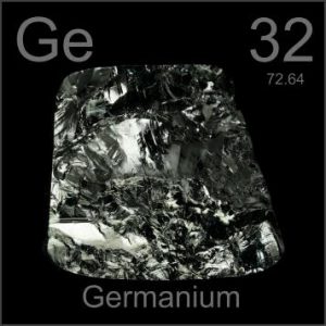
Germanium (Ge) is a chemical element that plays a pivotal role in the modern tech landscape, sitting with an atomic number 32 in the carbon group of the periodic table. This metalloid is characterized by its lustrous, hard, and grayish-white appearance, and it shares chemical similarities with its group neighbors, silicon and tin.
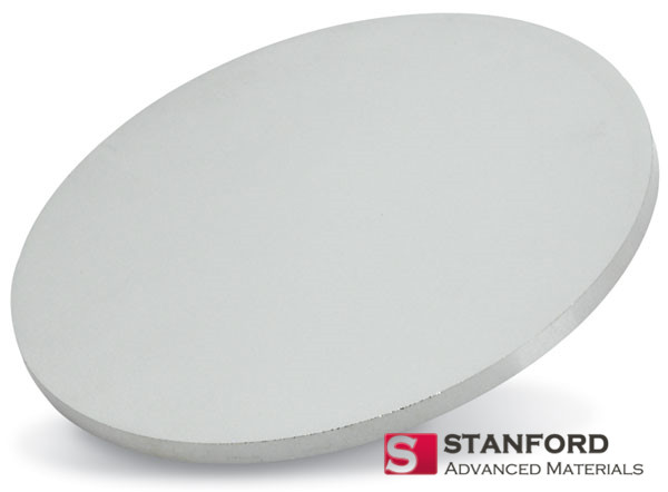
Germanium’s versatility is showcased through its ability to form a myriad of compounds, making it an invaluable resource in electronics, photonics, and more. Specifically, Germanium Sputter Targets represent a highly pure and refined form of this element, tailored for use in the sputtering process—a critical technique in the fabrication of electronic components, optical devices, and solar cells. These targets are essential for depositing thin, uniform layers of germanium onto various substrates, a step that is fundamental in the manufacture of semiconductors, fiber optic cables, and infrared optics.
A Closer Look at Its Unique Properties
Semiconductor Excellence
At the heart of germanium’s appeal as a semiconductor material lies its band gap of about 0.66 eV at room temperature, which is narrower than that of silicon. This narrow band gap facilitates the efficient movement of charge carriers (electrons and holes), enabling devices made from germanium to operate at lower voltages and higher speeds than their silicon counterparts. This characteristic is particularly advantageous in the design of transistors and integrated circuits where speed and power efficiency are paramount.
Optical Properties
Germanium’s optical properties are equally remarkable. It is transparent to infrared light, with a broad transmission range from about 2 to 14 µm, making it an essential material for applications in infrared optics.
This transparency allows germanium to be used in the production of lenses and windows for thermal imaging cameras, night vision devices, and other systems relying on infrared radiation. The ability to efficiently transmit infrared light also makes germanium an ideal material for fiber optic applications, where it is used to modify the refractive index of silica-based fibers, enhancing signal transmission over long distances.
Mechanical and Thermal Characteristics
In addition to its electronic and optical properties, germanium also possesses notable mechanical and thermal characteristics. It has a high melting point (approximately 938°C or 1720°F) and exhibits good thermal conductivity, making it suitable for applications that require stability under varying thermal conditions. These properties ensure that devices and components can maintain performance across a broad range of temperatures, a critical factor in aerospace and military applications.
| Property Category | Property | Impact/Application |
|---|---|---|
| Semiconductor Excellence | Band Gap: ~0.66 eV at room temperature | – Enables devices to operate at lower voltages and higher speeds.
– Advantageous for transistors and integrated circuits. |
| Optical Properties | Transparency: 2 to 14 µm infrared light | – Essential for infrared optics applications.
– Used in thermal imaging, night vision devices, and fiber optic cables. |
| Mechanical Characteristics | High Melting Point: ~938°C (1720°F) | – Suitable for applications requiring stability under thermal conditions.
– Important for aerospace and military applications. |
| Thermal Characteristics | Good Thermal Conductivity | – Ensures devices and components maintain performance across temperature ranges.
– Critical for durable electronic and mechanical systems. |
The Essence of Sputtering
Sputtering emerges as a foundational technique within the domain of physical vapor deposition (PVD), a process that has revolutionized the way thin material films are deposited onto substrates. This advanced method harnesses high-energy particles, typically ions sourced from an inert gas such as argon, to dislodge atoms or molecules from a solid target material, like germanium, under vacuum conditions.
The fundamental mechanics of sputtering involve accelerating these ions into the target material with sufficient energy to overcome the bonds holding the target’s atoms in place. Upon collision, a momentum transfer occurs, ejecting target atoms into the vacuum where they can then condense onto a nearby substrate, layer by layer, forming a thin film.
Detailed Mechanics of Sputtering
The process begins in a sputtering chamber, where the target material is positioned opposite the substrate. The chamber is evacuated to create a high-vacuum environment, minimizing the presence of unwanted gases that could interfere with the deposition process.
An inert gas, often argon, is then introduced at a controlled pressure. An electric field is applied to ionize the gas, turning it into a plasma—the fourth state of matter.
This plasma contains positively charged ions and free electrons. The positive ions are attracted to the negatively charged target due to the electric field, colliding with the target’s surface with high energy.
Diverse Applications of Germanium Sputter Targets
Semiconductor Devices
Germanium’s role in the semiconductor industry is both historic and crucial. As a semiconductor material, germanium boasts high carrier mobility, which translates to faster electron transport within devices. This property is particularly beneficial for fabricating transistors, diodes, and integrated circuits that operate at high speeds while consuming less power. Germanium’s compatibility with silicon and other semiconductor materials allows for the creation of heterojunction devices, which are key to enhancing the performance of a wide array of electronic gadgets.

Fiber Optics
The use of germanium-doped silica in the core of fiber optic cables is a testament to germanium’s versatility and importance in communication technologies. By adjusting the refractive index of the glass, germanium enables the efficient transmission of light signals over long distances with minimal loss, which is foundational to the internet and telecommunications networks around the globe.
Infrared Optics
Germanium’s transparency to infrared light makes it an invaluable material in the manufacture of lenses and windows for thermal imaging devices, night vision equipment, and other infrared applications. The ability to see beyond the visible spectrum opens a range of possibilities for security, surveillance, navigation, and medical imaging technologies.
Solar Cells
The photovoltaic industry benefits from germanium’s use as a substrate for the epitaxial growth of III-V semiconductors, which are crucial for developing high-efficiency multijunction solar cells. These cells are capable of converting a broader spectrum of sunlight into electrical energy, making them especially useful in space applications and in concentrated photovoltaic systems where maximizing energy conversion efficiency is paramount.
Innovations and Future Directions
The continuous evolution of sputter deposition technology is driven by the quest for more efficient, cost-effective, and environmentally friendly production methods. Innovations in the development of germanium alloy targets, which incorporate elements like gallium or arsenic, have the potential to further enhance the electrical and optical properties of thin films, opening new avenues for device optimization. Moreover, advancements in thin film deposition technologies promise even greater control over film characteristics, enabling the engineering of materials with tailor-made properties for specific applications.
Conclusion
In summary, Germanium Sputter Targets are at the heart of numerous technological advancements and are integral to the ongoing development of electronic, optical, and energy-harvesting devices. Their purity, adaptability, and the precision they bring to the sputtering process make them irreplaceable in high-tech manufacturing.
As we move forward, the continued innovation in sputter target composition, along with advancements in deposition techniques, will undoubtedly unlock new potentials in the efficiency and functionality of devices across a broad spectrum of industries. The strategic importance of germanium in enabling these advancements underscores the material’s enduring value and the need for sustained research and development efforts in this field.
Click to Inquiry High Quality Germanium Target


