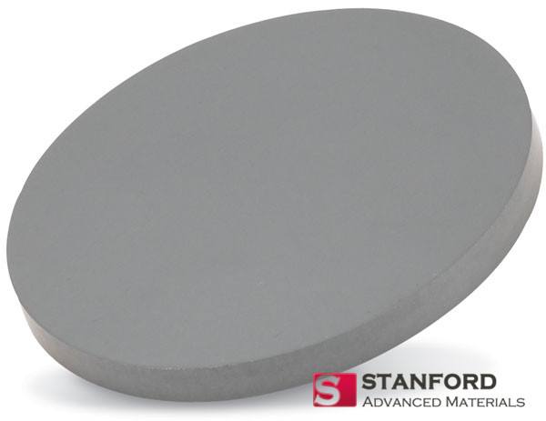
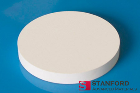
Our Zinc Sulfide (ZnS) Planar Sputtering Targets are fabricated from high-purity ZnS, a versatile II-VI compound semiconductor prized for its exceptional infrared transparency and luminescent properties. These targets enable the deposition of high-quality ZnS thin films used as key components in infrared optics, electroluminescent displays, and as buffer layers for advanced semiconductor heterostructures.
| Material | Zinc Sulfide (ZnS) |
| Typical Purity | ≥ 99.99% (4N) |
| Form & Shape | Planar Sputtering Target (Rectangular/Disc) |
| Crystal Phase | Cubic (Zinc Blende) and/or Hexagonal (Wurtzite) |
| Key Properties | Wide Bandgap (~3.7 eV) | Excellent IR Transparency (8-12 µm) | Efficient Luminescence |
| Key Advantage | Provides a high-purity source for depositing films with outstanding optical clarity in the infrared spectrum and efficient light emission properties for display technologies. |
Key Advantage: Enables deposition of high-quality ZnS films with low absorption and scattering losses, making them ideal for multi-layer anti-reflection coatings in IR systems and as the active layer in thin-film electroluminescent (TFEL) devices.
Customization: Purity (99.99% to 99.9999%), stoichiometry (Zn:S ratio), dimensions, and crystal phase emphasis are fully customizable to meet specific optical or electronic performance requirements.
Primary Applications: Anti-reflection and protective coatings for infrared windows and lenses; active luminescent layer in AC-driven TFEL displays; buffer layer for growing other II-VI semiconductors (e.g., CdTe, HgCdTe); passivation layers for optoelectronic devices.
Technical specifications for sputtering high-performance ZnS optical and electronic films.
| Parameter | Specification / Details |
|---|---|
| Material | Zinc Sulfide (ZnS) |
| Typical Purity | ≥ 99.99% (4N) |
| Crystal Phase | Primarily Cubic (Zinc Blende, preferred for IR optics); Hexagonal (Wurtzite) available |
| Stoichiometry | Nominally 1:1 Zn:S. Slightly Zn-rich or S-rich compositions available to influence conductivity and optical properties. |
| Density | ~4.09 g/cm³ (Theoretical, cubic phase) |
| Bandgap | ~3.54 – 3.91 eV (Direct, phase-dependent) |
| Transparency Range | ~0.4 – 14 µm (Visible to Long-Wave IR) |
| Refractive Index (@10 µm) | ~2.2 |
| Standard Shape | Planar – Rectangular, Circular (Disc) |
| Dimensions | Fully Customizable (Thickness, Width, Length, Diameter) |
| Surface Finish | Fine-ground and polished for uniform sputtering and minimal particulate generation |
| Bonding Option | Available bonded to metal backing plates (Cu, Mo) using conductive epoxy or specialized bonding for RF sputtering |
| Manufacturing Method | Hot Pressing or Chemical Vapor Deposition (CVD) of high-purity powder to achieve high density and transparency |
| Conductivity | Insulating – Requires RF Sputtering or pulsed-DC reactive sputtering from metallic Zn in H₂S/Ar |
| Quality Documentation | Certificate of Analysis with purity, phase (XRD), and optical grade verification |
ZnS is a cornerstone material for infrared optical systems due to its unique combination of properties:
ZnS doped with manganese (Mn) is the seminal phosphor material for TFEL displays:
ZnS serves important roles in compound semiconductor device fabrication:
As an insulating material, ZnS requires specific sputtering approaches:
Stanford Advanced Materials employs stringent controls for optical-grade ZnS targets:
To receive a formal quotation or technical consultation, please provide: