(949) 407-8904 Mon - Fri 08:00 - 17:00 1940 East Deere Avenue, Suite 100, Santa Ana, CA 92705, USA

ST11210 Silicon Carbide (SiC) Planar Sputtering Target

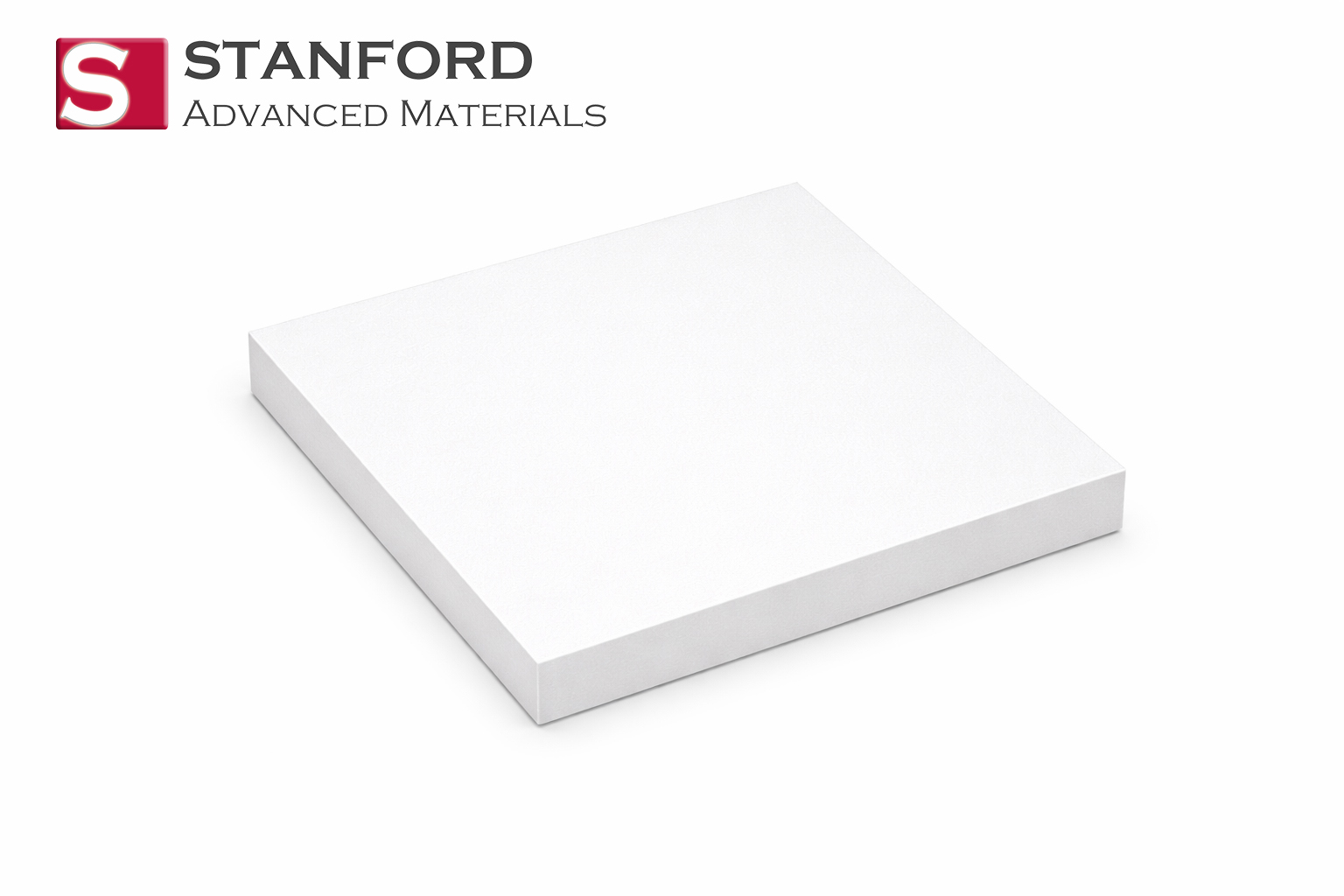
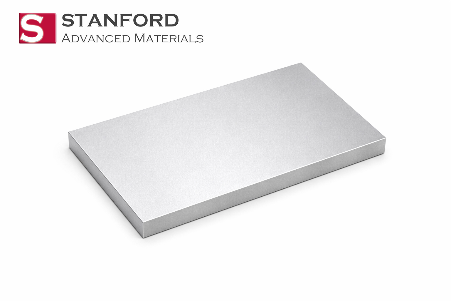
Our Silicon Carbide (SiC) Planar Sputtering Targets are engineered in a rectangular planar geometry for optimal compatibility with standard magnetron sputter systems. This configuration ensures uniform plasma distribution and erosion, which is critical for depositing consistent, high-performance films that offer exceptional hardness, chemical inertness, and thermal stability for protective coating applications.

Material Silicon Carbide (SiC)
Form Factor Rectangular Planar Target
Purity ≥ 99.9% (3N) Standard
Key Properties Extreme Hardness, High Thermal Conductivity, Chemical Inertness

Key Advantage: The planar design combined with a dense, phase-pure ceramic microstructure enables stable, low-arcing RF sputtering, producing films with superior adhesion and uniformity for demanding environments.

Customization: Planar dimensions (length, width, thickness) are fully customizable to fit your specific sputter gun or chamber requirements. Bonding to backing plates is available.

Typical Applications: Planar magnetron sputtering of wear-resistant coatings on tools, corrosion barriers for industrial components, and diffusion barrier layers in semiconductors.


Description

Complete Technical Specifications

For detailed evaluation and procurement (Product Code: ST11210).

Parameter Specification / Typical Value
Material Silicon Carbide (SiC)
Target Geometry Planar (Rectangular)
Purity (Standard) ≥ 99.9% (3N)
Crystal Phase α-SiC (Hexagonal) or β-SiC (Cubic) Available
Density ≥ 3.15 g/cm³ (High, >97% Theoretical)
Knoop Hardness (Film) ~2500 – 3000 kg/mm²
Thermal Conductivity ~80 – 120 W/(m·K)
Planar Dimensions Fully Customizable (Thickness, Length, Width)
Standard Shape Rectangular Planar
Sputtering Method RF Planar Magnetron Sputtering (Recommended)
Bonding Options For planar bonding to cooled backing plates
Certification CoA with XRD Phase Analysis and ICP/OES impurity data

Technical & Application Notes

1. Advantages of the Planar Target Geometry for SiC

The rectangular planar form is the industry standard for magnetron sputtering sources due to:

  • Uniform Erosion Profile: Promotes even material utilization and consistent deposition rates over the target’s lifetime.
  • Optimized Plasma Confinement: Works efficiently with planar magnetrons to create a dense plasma above the target surface, enhancing sputtering efficiency.
  • Ease of Integration & Bonding: The flat back surface allows for reliable, full-area bonding to a water-cooled backing plate, which is critical for managing heat during the RF sputtering of SiC.
  • Compatibility: Designed to fit most commercial planar sputter source assemblies without modification.

2. The Ultimate Protective Coating for Extreme Environments

SiC films deposited from our planar targets offer a unique combination of properties for surface engineering:

  • Wear & Abrasion Resistance: Applied via planar magnetron sputtering to cutting tools, molds, and bearings to drastically extend service life.
  • Corrosion & Oxidation Protection: Used as a barrier coating on metallic components in chemical and aerospace sectors.
  • Automotive & Aerospace Components: Deposited on piston rings or turbine blades to enhance durability under high stress.

3. Critical Semiconductor & Advanced Electronics Applications

Beyond mechanical protection, SiC’s electronic properties are leveraged:

  • Diffusion Barrier Layers: Thin, uniform SiC films from planar targets prevent intermigration in integrated circuits.
  • Hard Mask for Etching: SiC’s etch selectivity makes it an excellent hard mask material in advanced semiconductor patterning.

4. Sputtering Process Considerations for SiC Planar Targets

Sputtering from a SiC planar ceramic target requires specific process adaptations:

  • RF Power Required: As an insulating material, RF planar magnetron sputtering is the standard technique.
  • High-Density Planar Target Critical: Minimizes porosity, reducing arcing and particles.
  • Effective Cooling: The planar bonding interface must be optimized for maximum heat transfer to the cooling plate.

Quality Assurance

For SiC planar targets, we ensure:

  1. Planarity & Surface Finish: Precise machining to ensure flatness and a smooth surface for uniform bonding and sputtering.
  2. X-ray Diffraction (XRD): Verifies crystal phase and purity.
  3. Archimedes Density Measurement: Ensures high density for performance.
  4. Microstructural Analysis (SEM): Inspects grain uniformity.

Why Stanford Advanced Materials (SAM)

  • Precision-Engineered Planar Geometry: Our targets are machined to exacting tolerances for optimal fit and performance in your sputter source.
  • Advanced Ceramics Expertise: We master the sintering of high-performance planar ceramic targets like SiC.
  • Focus on Functional Properties: We deliver targets optimized for the final coating’s hardness, density, and stability.

Request More Information

Specify Your Planar Sputtering Needs
To provide an accurate quote, please specify:

  1. Your planar magnetron sputter source model or required target dimensions (Length x Width x Thickness).
  2. Primary application and key film property goals.
  3. Preferred SiC crystal phase (α or β) and purity grade.
Request a Quote