Thin Film Coating Technologies: Sputtering vs. Thermal Evaporation
Introduction
Thin film coatings are a critical component of various industries, from microelectronics to optics. Two prominent techniques for depositing these thin films are sputtering and thermal evaporation. Let’s compare these two technologies to understand their strengths and applications.
Sputtering: Precision and Versatility
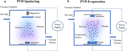
Sputtering is a physical vapor deposition (PVD) technique that involves the removal of atoms from a solid target material and their deposition onto a substrate.
- –Process: High-energy plasma dislodges target atoms, forming the film on the substrate.
- –Control: Sputtering offers precise control over deposition with adjustable parameters like plasma power and gas pressure.
- –Uniformity: It results in highly uniform and conformal films, ideal for applications like semiconductor manufacturing.
- –Materials: Sputtering is versatile and compatible with various materials, including metals, ceramics, and compounds.
- –Applications: Commonly used in integrated circuits, solar cells, and optical coatings, it’s valued in many industries.
Related reading: Exploring the Advantages and Disadvantages of Sputtering
Thermal Evaporation: Purity and Precision
Thermal evaporation, also known as vacuum evaporation, involves the sublimation of a material and its condensation onto a substrate.
- –Process: In thermal evaporation, the source material is heated in a vacuum chamber until it vaporizes. The vaporized material condenses onto the substrate, forming a thin film.
- –Control: While thermal evaporation provides good control over deposition rates, it may not offer the same level of precision as sputtering. Factors like temperature and deposition time impact film properties.
- –Uniformity: Achieving uniformity in thermal evaporation can be more challenging, particularly for large or complex substrates. However, with careful process control, uniform coatings can be obtained.
- –Materials: Thermal evaporation materials can typically be sublimated without decomposition, such as metals and some organic compounds. It may not be as versatile as sputtering in terms of material options.
- –Applications: Thermal evaporation is often employed in applications where a high degree of purity is required, such as organic light-emitting diodes (OLEDs) and organic photovoltaic cells. It is also used in the deposition of metal contacts and mirrors.
Choosing the Right Technique
Selecting sputtering or thermal evaporation depends on specific application needs. Sputtering suits microelectronics and optical coatings, offering precise control and uniformity. Thermal evaporation excels where material purity is paramount, as in organic electronics. In some cases, a combination, known as co-evaporation, leverages their strengths.
Understanding these techniques’ unique advantages is crucial for choosing the best thin film deposition method for a project. Stanford Advanced Materials (SAM) is a prominent supplier of diverse sputtering targets and evaporation materials. Our extensive range of evaporation materials include foils, wires, pellets, tablet, etc., and we welcome customization to meet specific needs. If you are interested in any of our products or require customized solutions, please feel free to send us an inquiry.


