| Chemical Formula | GaN |
| Catalog No. | ST0883 |
| CAS Number | 25617-97-4 |
| Purity | 99.9%, 99.95%, 99.99%, 99.995%, 99.999% |
| Shape | Discs, Plates, Column Targets, Step Targets, Custom-made |
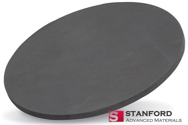
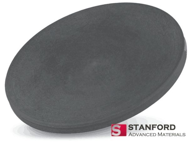
The Gallium Nitride Sputtering Target is available in various forms, purities, sizes, and prices. Stanford Advanced Materials (SAM) offers high-quality Gallium Nitride Sputtering Targets at the most competitive prices.
Gallium Nitride Sputtering Targets consist of a solid piece or disk made primarily of gallium nitride (GaN), which is a compound semiconductor material. GaN is known for its wide bandgap, high thermal conductivity, and good electrical properties, making it suitable for applications in various electronic devices, such as LEDs, power electronics, and wireless communication systems.
Gallium is a chemical element originated from France (with the Latin name Gallia). It was first mentioned in 1875 and observed by P. E. L. de Boisbaudran. The isolation was later accomplished and announced by P. E. L. de Boisbaudran. “Ga” is the canonical chemical symbol of gallium. Its atomic number in the periodic table of elements is 31 with location at Period 4 and Group 13, belonging to the p-block. The relative atomic mass of gallium is 69.723(1) Dalton, the number in the brackets indicating the uncertainty.
Related Product: Gallium Sputtering Target
| Compound Formula | GaN |
| Molecular Weight | 83.73 |
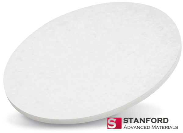
| Appearance | Yellow Target |
| Melting Point | >1600℃ |
| Density | 6.15 g/cm3 |
| Available Sizes | Dia.: 1.0″, 2.0″, 3.0″, 4.0″, 5.0″, 6.0″
Thick: 0.125″, 0.250″ |
Gallium Nitride Sputtering Target is known for its wide bandgap, high thermal conductivity, and good electrical properties, making it suitable for applications in various electronic devices, such as LEDs, power electronics, and wireless communication systems.
Our Gallium Nitride Sputtering Targets are carefully handled during storage and transportation to preserve the quality of our products in their original condition.
SAM’s Gallium Nitride Sputtering Targets are available in various forms, purities, and sizes. We specialize in producing high purity physical vapor deposition (PVD) materials with the highest possible density and smallest possible average grain sizes for use in semiconductor, chemical vapor deposition (CVD) and physical vapor deposition (PVD) display and optical applications. Get an inquiry right now.
Submit your review | |