Remarkable Benefits of Silicon Sputtering Targets
Introduction
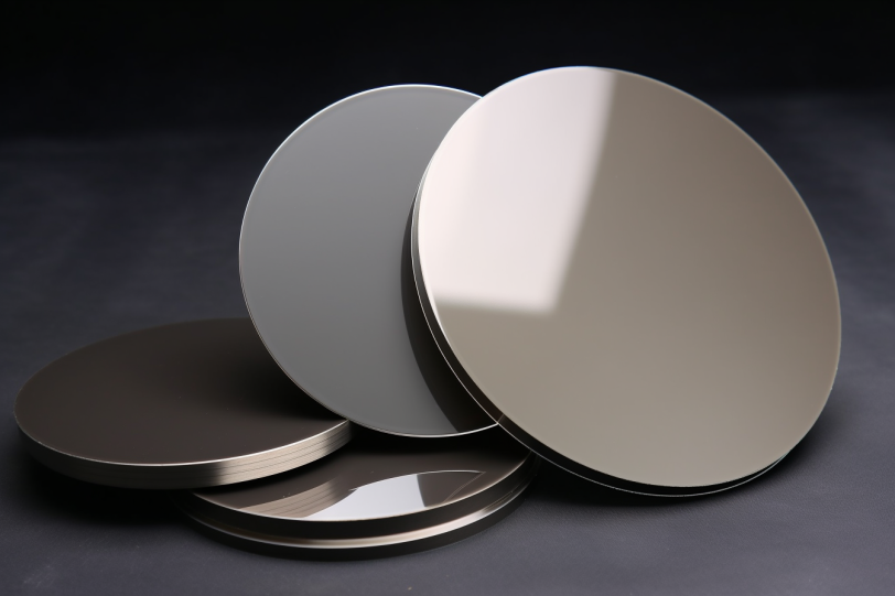
Silicon sputtering targets are one of the cornerstones in the field of thin film deposition, offering huge advantages to industries such as semiconductors, solar panels, and advanced coatings. This article takes an in-depth look at the exceptional benefits and properties of silicon sputtering targets, revealing why they are ideal for achieving superior thin film deposition results.
Exceptional Purity and Consistency
The purity and consistency of the raw material is critical during thin film deposition, and silicon sputtering targets excel in this regard. The exceptional purity of silicon targets ensures that the deposition process is not hindered by impurities. At the same time, the composition of these targets has a high degree of uniformity and consistency, enabling precise control of film properties, thereby improving device performance and reliability. The exceptional purity and consistency of silicon sputtering targets finds applications in everything from advanced microelectronics to complex solar cells.
Optimal Performance with Precise Dimensions
Optimum performance in thin film deposition requires precise dimensions of the sputtering target. SAM’s sputtering targets can be engineered to exact specifications for customers’ projects, ensuring they are perfectly matched to specific coating systems. This helps achieve uniform film thickness, minimizes defects and improves overall product yield.
Exceptional Thermal Conductivity
Thermal management is critical in numerous industries, including electronics and energy conversion. Silicon sputtering targets boast outstanding thermal conductivity, efficiently dissipating heat during the sputtering process. This superior thermal performance enables higher power densities, lower operating temperatures, and enhanced device reliability. With silicon sputtering targets, you can push the boundaries of power electronics, photovoltaics, and thermal management solutions, all while maintaining stability and prolonging the lifespan of your devices.
High-Density Structure for Longevity
Target durability and lifetime are critical to any sputtering process. SAM’s silicon sputtering targets are designed with a high-density structure that ensures excellent mechanical strength and resistance to cracking or fracture during deposition. This extends target life, minimizes downtime and maximizes productivity. Whether you’re in mass production or cutting-edge research, silicon sputtering targets provide the robustness needed to withstand demanding processes and deliver consistent performance over extended periods of time.
Versatility in Size and Configuration
SAM’s silicon targets are available in a variety of sizes and configurations to meet different thin film deposition requirements. From small substrates to large-area coatings, manufacturers can find precisely tailored targets for their specific deposition systems. Whether you need round or rectangular targets, monocrystalline or polycrystalline silicon, a wide range of options ensures the highest precision and efficiency for your thin film deposition work. This versatility allows greater flexibility in product design and customizability to meet the unique needs of various applications.
Conclusion
Silicon sputtering targets have revolutionized thin film deposition, empowering industries with advanced materials and enhanced manufacturing capabilities. The unmatched purity, precise dimensions, exceptional thermal conductivity, high-density structure, and versatile configurations of silicon sputtering targets unleash new possibilities in semiconductor fabrication, solar energy, and beyond. Embrace these remarkable benefits, and take your thin film deposition processes to unprecedented levels of excellence.
For more information about sputtering targets and their applications, please visit our homepage.


