Benefits of Palladium Sputter Targets in Thin Film Deposition
See our Palladium Sputter Targets
Introduction
Palladium (Pd) is a highly sought-after metal for thin film deposition due to its unique properties. One popular method for depositing Pd thin films is through the use of sputtering targets. In this article, we will explore the benefits of using palladium sputter targets for thin film deposition and their applications in various industries.
Properties of Palladium
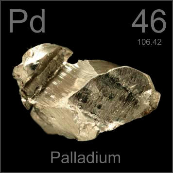
Palladium is a chemical element with the symbol Pd and atomic number 46. It is a rare and lustrous silvery-white metal that belongs to the platinum group of metals. It is both ductile and malleable, and has a high melting point and density. Palladium is well-known for its resistance to corrosion, oxidation, and chemical reactions, making it ideal for use in a wide range of industrial and commercial applications. It is also highly conductive, which makes it especially useful in electronics and other high-tech industries.
Sputtering Deposition and How It Works
Sputtering deposition is a process that involves the deposition of a thin film of material onto a substrate by bombarding a target material with high-energy ions. This bombardment causes the target material to erode, releasing particles that are then deposited onto the substrate. The sputtering process is used in a wide range of applications, including thin film deposition, surface modification, and microfabrication. To use sputtering technology for palladium thin film deposition, palladium sputter targets must be used.
Advantages of Palladium Sputter Targets
There are several advantages to using palladium sputter targets for thin film deposition. One of the biggest benefits is the ability to produce consistent, high-quality thin films of palladium. The sputtering process allows for very precise control over the deposition rate, which means that the thickness of the thin film can be controlled to within a few nanometers. This level of precision is difficult to achieve with other deposition methods, such as electroplating or evaporation. Additionally, palladium sputter targets are cost-effective compared to other precious metals like gold or platinum.
Applications of Palladium Thin Films
Electronics Industry
In addition to being used in magnetic storage media, palladium thin films are also used in other areas of the electronics industry. For example, they are used as electrodes in capacitors, as interconnects in integrated circuits, and in the fabrication of thin film transistors. Furthermore, palladium thin films are commonly used in microelectromechanical systems (MEMS) and nanoelectronics.
Gas Sensors and Detectors
Palladium thin films are commonly used in gas sensors and detectors due to their high reactivity with certain gases, such as hydrogen. In these applications, the palladium thin film acts as a sensing layer that detects the presence of the target gas. This can be used in a variety of settings, such as in automotive emissions control, industrial gas leak detection, and personal safety devices.
Catalysis
Palladium is widely used as a catalyst in chemical reactions due to its unique electronic structure, which allows it to bond with a wide variety of molecules. In particular, palladium is commonly used in organic synthesis reactions, such as Suzuki coupling reactions and Heck reactions. Palladium thin films are also used in catalysis for fuel cells, which convert chemical energy into electrical energy.
Biomedical Applications
Palladium thin films have potential applications in the biomedical field, particularly in implantable medical devices. For example, palladium thin films have been used as coatings on titanium implants to improve their compatibility with the body, reducing the risk of rejection or infection. Additionally, palladium thin films have shown promise in drug delivery applications, as well as in the detection of biomolecules such as glucose.
Conclusion:
Palladium sputtering targets offer a cost-effective and efficient method for depositing high-quality thin films of palladium for use in various industries. Their unique properties, along with sputtering technology, make them an attractive option for researchers and manufacturers looking to create reliable and consistent thin films for a variety of applications. With such broad applications, palladium sputter targets and thin films will continue to play an important role in the development of new products and technologies in the future.
For more information about sputtering targets and their applications, please visit our homepage.
Inquiry SAM's Pd Sputter Target


