Advancements in Indium Tin Oxide Nanotechnology
Introduction
Indium Tin Oxide (ITO) has long been a stalwart in the realm of transparent conducting oxides, but recent strides in nanotechnology have ushered in a new era for this versatile material. This article looks at ITO nanotechnology, studying how making tiny structures is changing the way ITO works. This helps it do more things with new technologies.
Understanding ITO Nanotechnology
ITO, or Indium Tin Oxide, is renowned for its dual capability of permitting electrical flow while maintaining optical transparency. Researchers deeply appreciate its electrical conductivity and see-through quality, yet they aim for more refinement. This pursuit of enhancement leads them into the intricate realm of nanotechnology.
Nanotechnology involves the meticulous manipulation of materials at the atomic and molecular levels. It delves into the intricacies of working with components far smaller than the human eye can discern – an arena where atoms and molecules become the building blocks for scientific endeavors.
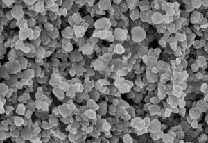
In the marriage of ITO and nanotechnology, scientists craft what are known as nanostructured materials. These intricate structures arise from the deliberate manipulation of particle size and arrangement. It’s akin to constructing with the tiniest, most sophisticated building blocks imaginable.
Why does this meticulous arrangement matter? The significance lies in the profound impact that the size and arrangement of these particles have on functionality. It’s akin to orchestrating those minuscule building blocks in precise harmony, ensuring optimal strength and efficacy. In the fusion of ITO and nanotechnology, these nanostructured materials emerge as the unsung heroes, elevating the effectiveness of ITO to new heights.
Imagine possessing control over the behavior of each diminutive piece – akin to wielding a magical wand, albeit on a microscopic scale. This level of precision empowers scientists to elevate ITO’s performance to unprecedented levels. The objective is not merely improvement; it’s about achieving the pinnacle of excellence.
As we traverse the boundless possibilities within the realm of ITO and nanotechnology, it transcends a mere exploration of the minuscule. Rather, it is a deliberate endeavor, recognizing that these infinitesimal intricacies hold the key to unlocking the true potential of ITO. It mirrors the revelation of the inner workings of a superhero suit – comprehending the nuances of each component contributes to the creation of something extraordinary.
Therefore, when delving into the synergy of ITO and nanotechnology, the discourse extends beyond the laboratory setting. It unfolds as an odyssey into the microscopic, a journey where precision transforms materials into extraordinary entities. The expedition into nanotechnology is synonymous with discovering an uncharted realm where the minutest details wield the most profound influence.
Nanotechnology Techniques for ITO
Several nanotechnology techniques are employed to enhance ITO properties:
- Nanostructuring through Sputtering:
- Sputtering is a method to apply thin films of ITO. By carefully managing the conditions during this process at the tiny nanoscale, scientists can make nanostructured ITO films. This helps improve how well they conduct electricity and how transparent they are.
- Chemical Vapor Deposition (CVD):
- CVD processes at the nanoscale enable the growth of well-defined ITO nanostructures. This precise control during the deposition process helps in creating nanomaterials that perform exceptionally well.
- Sol-Gel Synthesis:
- Using sol-gel techniques makes it possible to create ITO nanoparticles with specific properties. The key here is to control the size and arrangement of particles, which is vital for making ITO that is both conductive and transparent.
Enhanced Properties of Nanostructured ITO
Nanostructured ITO brings improved properties compared to its larger form:
1. Better Electrical Conductivity:
At the nanoscale, Nanostructured ITO steps up its game. It reduces grain boundaries and defects, giving electrons more room to move. This boost in electron mobility means Nanostructured ITO conducts electricity even better. This is a big deal for applications that need super-efficient see-through conductors.
2. Tunable Optical Transparency:
Nanostructuring lets scientists play with ITO’s bandgap, which is like the energy jump electrons make. It’s a bit like adjusting a musical instrument to get just the right note. With this control, researchers can fine-tune how see-through Nanostructured ITO is. This flexibility is great for gadgets that need specific transparency levels, like those cool devices with lots of lights.
3. Flexibility and Bendability:
Nanostructured ITO films are like the acrobats of electronics. Because of their special properties at the nanoscale, they can bend and stretch. Imagine a super-thin sheet of material that’s as flexible as a gymnast. This makes Nanostructured ITO a promising player in the world of flexible electronics, where gadgets can twist and turn without breaking.
Applications of Nanostructured ITO
The rise of nanostructured ITO has opened doors to various applications across different fields:
1. Flexible Displays:
Nanostructured ITO is like the superhero of flexible displays. It perfectly fits the need for screens that can bend and twist. Imagine a phone that folds in half or a watch that wraps around your wrist – that’s where nanostructured ITO comes in. It’s a crucial part of making screens that can flex without breaking, like the ones in foldable phones and wearable gadgets.
2. Next-Generation Solar Cells:
When it comes to solar power, nanostructured ITO is a game-changer. It steps up the game in solar cell technology, making sunlight absorption and electron movement much better. This boost in efficiency is like upgrading from a regular bike to an electric one. Nanostructured ITO contributes to making thin-film solar cells work better, pushing us towards more sustainable and efficient solar energy.
3. Nanoelectronics and Quantum Devices:
Nanostructured ITO isn’t just limited to screens and solar cells; it’s making waves in the world of super-small electronics. Its amazing electrical properties make it a strong candidate for tiny electronic devices and cutting-edge quantum technologies. Think of it like fitting a powerful engine into a small car – nanostructured ITO is paving the way for exciting innovations in quantum dots and nanoscale electronics. This could lead to breakthroughs in how we build and use electronics in the future.
Challenges and Future Prospects
While we’re making good progress, it’s still tough to produce a lot of nanostructured ITO and make sure it stays stable over time. Researchers are actively exploring novel nanotechnology approaches and alternative materials to address these challenges.
The prospects for ITO nanotechnology are intriguing, with ongoing research poised to unlock new dimensions of its potential. As innovations continue, the applications of nanostructured ITO are expected to proliferate, contributing to the evolution of transparent conducting oxides in the nanotechnology era.
Conclusion
The marriage of ITO and nanotechnology marks a transformative phase in the realm of transparent conducting oxides. Nanostructured ITO, with its enhanced electrical conductivity, tunable optical transparency, and adaptability to flexible electronics, is spearheading advancements in various industries. Scientists are researching how ITO and nanotechnology can combine to make see-through conductors for future technologies.


