Major Facts about Bismuth Sputtering Targets
Introduction to the Bismuth Sputtering Target
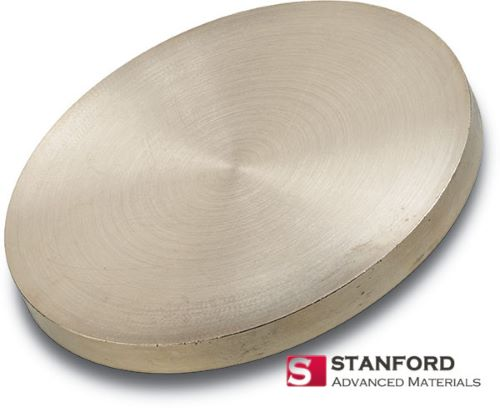
What is a bismuth sputtering target?
A bismuth sputtering target is a pure metal sputter target for film deposition. This product could be used to make thin films for multiple sectors, including semiconductors, glass coatings, LED, solar cells, and optical industries.
Properties of bismuth target
Bismuth (atomic symbol: Bi, atomic number: 83) is located in Period 6, Group 15, and p-block in the periodic table.
Bismuth is a brittle, lustrous, and crystalline metal with a red tinge over its white body. This metal is stable in air and water, and it is a poor conductor of heat and electricity. Bismuth is known as the most diamagnetic pure element. When compounds and composites are also taken into account, bismuth’s diamagnetism is second only to superconductors and compounds such as pyrolytic graphite.
Bismuth metal can be made into high-purity sputtering targets for film deposition, and it can be applied to numerous industries. Stanford Advanced Materials (SAM) specializes in producing high-purity bismuth sputter targets with the highest possible density, the smallest possible average grain sizes, and the smoothest possible surfaces.
Table 1 Bismuth Sputtering Target Specifications
| Material Type | Bismuth |
| Symbol | Bi |
| Color/Appearance | Lustrous Reddish White, Metallic |
| Melting Point | 2079 °C |
| Boiling Point | 1560 °C |
| Density | 9.747 g/cm3 |
| Sputter | RF |
| Type of Bond | Indium, Elastomer |
Manufacturing of Bismuth Sputtering Target
How to make a bismuth sputter target?
The manufacturing process of targets is quite complex. For more details, check the flow chart below.
Refining→Melting→Casting→Grain→Refinement→Cleaning
The process begins with refining metal ingots. Then, the bismuth metal ingots are melted and solidified. The next step is casting and shaping. A vacuum environment and inert gases are needed to reduce oxides. The whole process of manufacturing targets requires much attention and caution to obtain high-quality products.
Factors influencing the quality of the bismuth target
A number of factors can affect the quality of a sputtering target. Purity is quite crucial because impurities can lead to bad performance of the thin film. The grain size also matters. Smooth surface conditions are quite significant as well. Among them, the purity of bismuth sputtering targets is the most important factor. For example, semiconductor chips have high technical requirements for the purity of sputtered targets compared with other fields. Stanford Advanced Materials offers high-purity bismuth sputtering targets for consumers.
Film Deposition
What is film deposition?
A sputtering target is a material used to prepare thin films. The preparation process is called film deposition. Film deposition was discovered in 1852, and it was developed as a technique in 1920. Film deposition is now extensively used in modern manufacturing.
During the deposition process, atoms in electron beams or ion beams are ejected from the sputtering target to the substrate. Finally, a thin but valid film is formed for a variety of applications. With the very thin layers of material on it, the substrate could obtain enhanced properties, such as unique electrical, mechanical, or optical qualities.
Factors included in a film deposition process
A complete film deposition process includes several factors. They are:
- Sputter Targets: It is the source material. Sputtering targets could be made from metals, alloys, and ceramics. Metals are often used as sputtering target materials for their strong and durable features. Stanford Advanced Materials is an international supplier of metal targets, alloy targets, ceramic targets, etc.
- Substrates: It is the destination for the atoms. Atoms gathered on the surface of the substrate and form a thin coating The thin film can enhance the characteristics of the substrate.
- Backing Plates: The film deposition process would be more solid with the help of backing plates. They are employed for assistance if there is any cracking, warping, or other damage. Stanford Advanced Materials offers Indium Bonding, Elastomer Bonding, and related customer services for bismuth sputtering targets.
- Inert Gases: Argon (Ar) and other inert gases are used to protect the materials in reaction. The void between the sputter targets and the substrates is usually filled with such inert process gases.
2 types of film deposition
Thin film deposition can be divided into two types: chemical vapor deposition (CVD) and physical vapor deposition (PVD). The chemical deposition process prepares a thin film by reacting, and it is used for materials with low melting points. The physical vapor deposition process makes thin coatings by heating and condensing, and it is used for materials with high melting points, such as metals and semiconductors. Stanford Advanced Materials has the best team and support to give you high-quality sputtering targets and thin films through the film deposition process.
Applications of Bismuth Target and Film Deposition
Nowadays, there are lots of daily products with thin layers made through the film deposition process. Bismuth sputtering targets and thin coatings are commonly used in manufacturing semiconductors and computer chips. These products offer multiple benefits for the substrate material. Commonly, these benefits involve enhanced durability, improved optical transmission, better electrical insulation, etc. With these improved features, a bismuth sputtering target is utilized in glass coating fields, wear-resistant materials, and other industries.
Related Products
Stanford Advanced Materials (SAM) offers high-purity bismuth sputtering targets of all shapes and configurations. The typical thicknesses of these targets include 0.125 inches and 0.25 inches. The company stocks circular targets. The typical diameters for them include 2 inches, 3 inches, 4 inches, 5 inches, and 6 inches. For further details, please check the tables below. Customized orders for commercial and research purposes are also welcomed. Send us an inquiry for more information, quick delivery, and competitive price.


