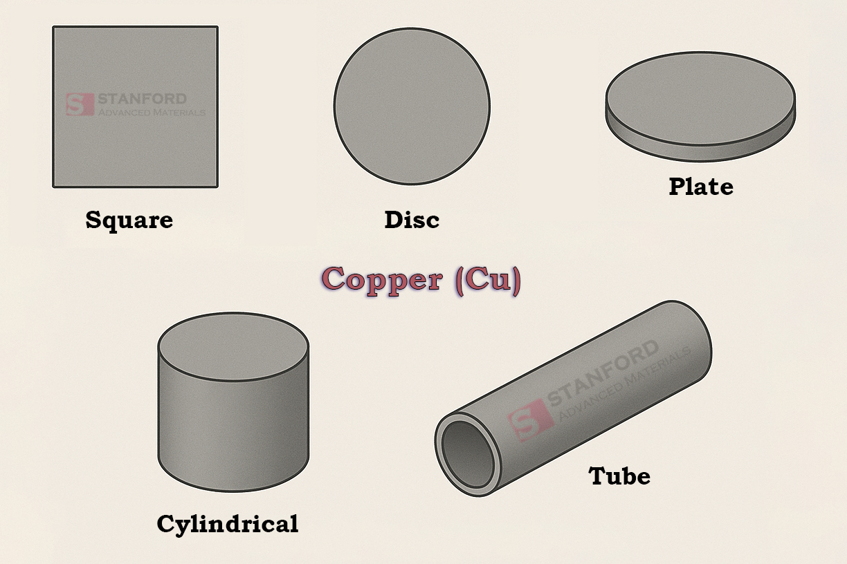
Copper sputter targets are used to deposit thin metal films on various substrates. They are chosen for their electrical and thermal conductivity, ductility, and adhesion properties. Thin films from copper appear in electronics, solar cells, displays, and decorative coatings. The shape and size of the target influence deposition uniformity and material usage. Target Shapes Planar...Continue Reading
Introduction Thin film deposition is an integral part of semiconductor chip production. Sputtering is perhaps the most established and reliable method of placing smooth films on wafers. Among all the materials that have been employed as targets, niobium stands out for its unique combination of electrical, thermal, and chemical properties that qualify it perfectly for...Continue Reading
Introduction The semiconductor industry is driving the technological revolution, fueling the progress of electronics, computing, and communications. As performance demands rise and chip dimensions continue to be reduced, the material employed for their manufacture must conform to increasingly stringent specifications. High-purity zirconium sputtering targets have become a flagship material for the industry, making it possible to form high-quality metal oxide thin films, gate material, as well as metal interconnect layers. This article...Continue Reading
Introduction One of SAM’s long-term clients—a major display panel manufacturer—was experiencing frequent production disruptions. The culprit: cracking and uneven wear in their ITO sputtering targets, used in the thin-film deposition process for smartphone and tablet displays. After reviewing the setup, SAM proposed switching to denser, more uniform ITO targets. That small change led to significant...Continue Reading
Introduction The semiconductor industry is the backbone of modern-day technology, powering everything from smart phones to artificially intelligent computers. As device sizes shrink and performance requirements expand, materials used in the semiconductor production process must be subjected to more demanding needs. High-purity Cr sputtering targets are now the focal material of this technology enabling high-toughness...Continue Reading
In the semiconductor industry, the demand for smaller, faster, and lower power devices has created a growing demand for advanced materials. High-purity vanadium (V) sputtering targets have also been found to be an essential material in overcoming some of the key challenges in chip manufacturing. With distinguishing features such as excellent conductivity, heat resistance, and...Continue Reading
The insatiable requirement for thinner, faster, and power-saving technologies has made the semiconductor industry one of the prime drivers of technological advancement. Behind the drive is a critical material: high-purity tantalum (Ta) sputtering targets. The targets are a critical ingredient in enabling next-generation semiconductor manufacturing processes, solving dire issues to chip reliability and performance. Tantalum...Continue Reading
1. Introduction Sputtering targets play a central role in physical vapor deposition (PVD) processes, forming the thin functional layers found in semiconductors, optical components, solar panels, and wear-resistant coatings. As industries continue to push for better film quality, consistency, and performance, the demand for advanced sputtering targets grows accordingly. In particular, refractory metals such as...Continue Reading
1. Introduction Refractory metals like tantalum (Ta) and niobium (Nb) play an increasingly important role in thin film technology, particularly for environments that demand both high-temperature stability and corrosion resistance. These two elements, known for their exceptionally high melting points and strong chemical inertness, have found widespread use in advanced protective coatings. As industries such...Continue Reading