| Material | CZTSSe |
| Purity | 99.9% |
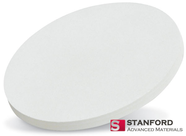
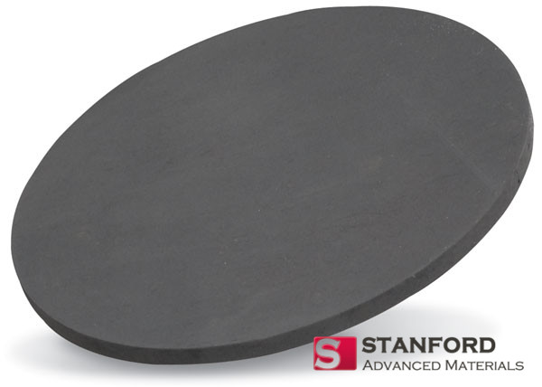
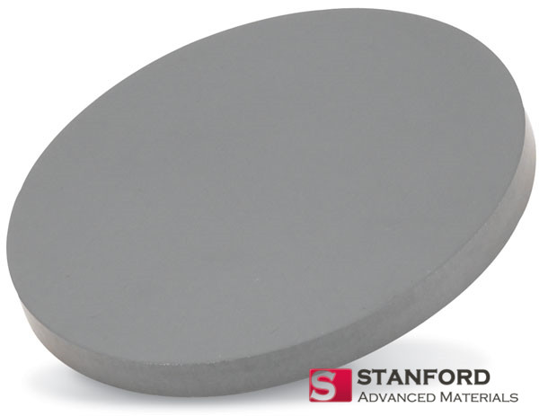
| Shape | Planar Disc |
Stanford Advanced Materials (SAM) introduces the Copper Zinc Tin Sulfide Selenide Target (CZTSSe), a superior quaternary compound designed for high-efficiency thin-film solar cells and advanced optoelectronic applications. This target ensures exceptional compositional uniformity and stable sputtering performance, making it ideal for cutting-edge photovoltaic technologies.
Note: The specifications provided are based on theoretical data. For tailored requirements and detailed inquiries, please contact us.
Related Products: Tin Sputtering Target, Sn, Tin Zinc Sputtering Target, Sn/Zn, Zinc Sputtering Target, Zn, Indium Zinc Oxide Sputtering Target, IZO, Copper Sputtering Target, Cu, Aluminum Copper Sputtering Target, Al/Cu, Antimony Sulfide Sputtering Target, Sb2S3, Barium Sulfide Sputtering Target, BaS, Selenium Sputtering Target, Se, Bismuth Selenide Sputtering Target, Bi2Se3
The Copper Zinc Tin Sulfide Selenide Target (CZTSSe) is a versatile quaternary semiconductor material celebrated for its adjustable bandgap, high optical absorption, and the use of earth-abundant elements. This makes CZTSSe an environmentally friendly and cost-effective alternative to conventional photovoltaic materials. As a sputtering target, CZTSSe ensures uniform chemical and structural properties, facilitating precise thin-film deposition with controlled stoichiometry.
By varying the ratio of sulfur to selenium, the bandgap of CZTSSe can be finely adjusted between 1.0 to 1.5 eV, optimizing solar energy conversion efficiency. Its high absorption coefficient (>10⁴ cm⁻¹) allows for the creation of thin yet highly efficient absorber layers. The target is manufactured with enhanced density and minimal porosity through techniques such as hot pressing or spark plasma sintering, which improve sputtering efficiency and ensure uniform film deposition. Additionally, CZTSSe is compatible with both vacuum and non-vacuum deposition methods and resists phase segregation during processing, making it ideal for scalable production of next-generation thin-film solar cells.
Our CZTSSe Targets are meticulously packaged to ensure their integrity during transit and storage. Depending on the size, smaller targets are securely placed in polypropylene (PP) boxes, while larger targets are shipped in custom-designed wooden crates. We prioritize customized packaging solutions, employing appropriate cushioning materials to provide maximum protection.
Packaging Options:
Q1: What is the primary advantage of using a CZTSSe sputtering target?
A1: CZTSSe comprises earth-abundant, non-toxic elements, making it a cost-effective and environmentally friendly alternative to traditional thin-film materials like CIGS.
Q2: Which deposition methods are compatible with CZTSSe targets?
A2: CZTSSe targets are suitable for use in both RF and DC magnetron sputtering systems. They can also be paired with post-deposition selenization or annealing processes to achieve the desired phase and crystallinity.
Q3: How is film quality maintained during deposition?
A3: Film quality is controlled by optimizing parameters such as substrate temperature, sputtering power, chamber pressure, and post-deposition annealing to prevent the formation of secondary phases.
| Property | CZTSSe Target | CIGS (CuInGaSe₂) | CdTe | Perovskite |
|---|---|---|---|---|
| Thermal Stability (°C) | Stable up to 600°C during annealing | Stable up to 550°C (limited by In volatility) | Stable up to 450°C (Cd toxicity concerns) | Stable up to 100°C (prone to degradation) |
| Mechanical Strength (MPa) | Residual stress: -0.27 GPa (with Ge layer); Flexural strength: ~300 | Moderate (brittle) | High (but brittle) | Low (flexible but fragile) |
| Sputtering Compatibility | High (compatible with CIGS industrial lines) | Industry-standard | Limited (requires handling of toxic Cd) | Requires specialized deposition |
| Environmental Resistance | Stable in humid conditions (with Ge/ZTO layers) | Moderate (moisture-sensitive) | Poor (risk of Cd corrosion) | Degrades in moisture and light |
Copper is a reddish-gold metal renowned for its exceptional electrical and thermal conductivity, corrosion resistance, and ductility. It is pivotal in electronics, energy systems, and alloy manufacturing.
Zinc is a bluish-white metal widely used for galvanizing steel to prevent rusting. It exhibits good corrosion resistance and is a vital component in numerous alloys, including brass and zinc-based semiconductors.
Tin is a soft, malleable metal with a low melting point and strong corrosion resistance. It is commonly used in soldering, coatings, and alloy applications, particularly in electronics and packaging industries.
Sulfur is a nonmetallic element available in several allotropic forms. It is essential for producing sulfide compounds and is extensively used in batteries, fertilizers, and as a dopant in semiconductor applications.
Selenium is a nonmetal with semiconducting properties, often utilized in solar cells, glassmaking, and electronics. It can substitute for sulfur in compounds to adjust optical and electronic properties.