Chemical Formula: Yb
Catalog Number: ST0056
CAS Number: 7440-64-4
Purity: 99.9%
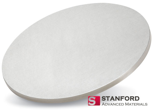
Shape: Discs, Plates, Column Targets, Step Targets, Custom-made
SAM’s Ytterbium Sputtering Targets are supplied in different purities, dimensions, and bonding options. Customized targets are available upon request.

Ytterbium is a rare earth metal with the symbol Yb and atomic number 70. It is a soft, silvery-white element belonging to the lanthanide series, first identified in 1878 in Ytterby, Sweden. The metallic form shows moderate density (6.9 g/cm³), low melting point (824 °C), and relatively high coefficient of thermal expansion. Ytterbium sputtering targets are valued in thin film deposition for their ability to form uniform coatings in optical, electronic, and decorative applications.
| Atomic Number | 70 |
| Density | 6.90 g/cm3 (near r.t.) |
| Color/Appearance | Silvery White, Metallic |
| Thermal Conductivity | 34.9 W/m.K |
| Melting Point | 824 °C |
| Boiling Point | 1196 °C |
| Coefficient of Thermal Expansion | 26.3 x 10⁻⁶/K |
| Z Ratio | 1.13 |
Other custom sizes and purities can be produced upon request.
Ytterbium sputtering targets are used in:
Each target is labeled and packaged for traceability and safe handling. Because ytterbium is chemically active in air, the targets are sealed in protective wrapping, with oil or vacuum packing applied to prevent oxidation during transport and storage.
Ytterbium sputtering targets are available in various forms, purities, sizes, and prices. We specialize in producing high-purity thin film deposition materials with the highest possible density and smallest possible average grain sizes for use in semiconductor, chemical vapor deposition (CVD), and physical vapor deposition (PVD) display and optical applications. Please send us an inquiry for current pricing on sputtering targets and other deposition materials not listed.
Submit your review | |
Our team recently purchased a Ytterbium sputtering target for use in our optical communication coating processes. The 2" diameter, 0.25" thick target arrived in perfect condition, and the 99.9% purity of the Yb was commendable. The target was compatible with both our RF and DC sputtering systems and provided a good sputtering yield. The quality of the thin films produced was stable and met all our application needs. We'll definitely be ordering again.
I got many from SAM for our chemistry lab and we use them for sputter deposition experiments. They're great for chemical projects and science for the students.