Zinc Oxide (ZnO) sputtering targets are a key material utilized during the deposition process known as magnetron sputtering. In the process, high-energy ions strike the target and eject zinc oxide atoms. The ejected atoms deposit themselves on substrates such as glass, forming a thin yet strong film. These Zinc Oxide films have been greatly helpful...Continue Reading
1. Introduction to Sputtering Targets Sputtering targets are significant commodities for thin-film industries like electronics, optics, and energy sectors. Simply put, a “sputtering target” is the target material utilized for sputtering, a form of physical vapor deposition (PVD). During the PVD process, atoms from a solid target are removed and ejected upon impact by high-energy...Continue Reading
Magnesium vs. Magnesium Oxide Targets – Which One Gets Better Film on Silicon? High-quality thin films play a big role in electronic and optical devices. Over the years, the choice of sputtering target has been shown to significantly influence film properties. When depositing magnesium oxide films on silicon, the selected target—either pure magnesium or magnesium...Continue Reading
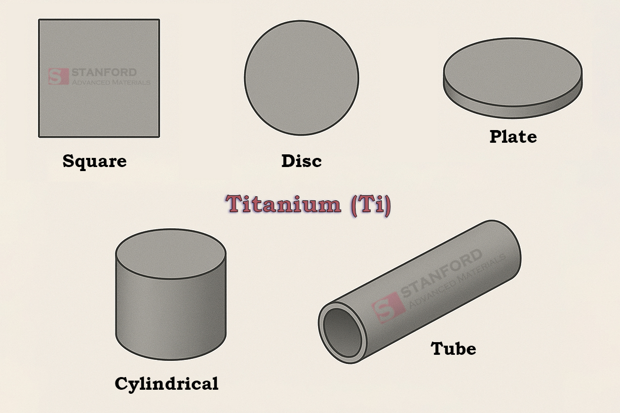
Titanium is a widely used material in thin film technology due to its high strength, corrosion resistance, and compatibility with a broad range of substrates. In sputtering, titanium targets are applied to deposit thin metallic films directly, or to form compound films such as titanium nitride (TiN) and titanium dioxide (TiO₂). These coatings are valued...Continue Reading
Copper sputter targets are used to deposit thin metal films on various substrates. They are chosen for their electrical and thermal conductivity, ductility, and adhesion properties. Thin films from copper appear in electronics, solar cells, displays, and decorative coatings. The shape and size of the target influence deposition uniformity and material usage. Target Shapes Planar...Continue Reading
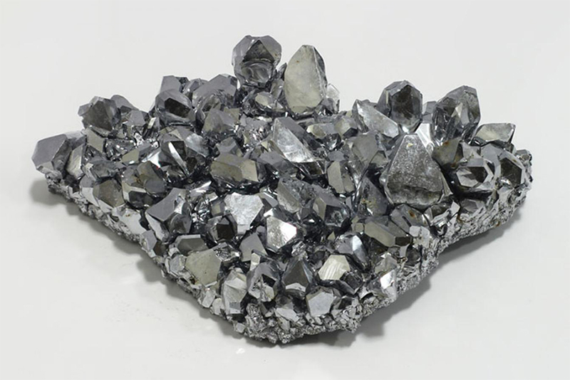
Introduction Thin film deposition is an integral part of semiconductor chip production. Sputtering is perhaps the most established and reliable method of placing smooth films on wafers. Among all the materials that have been employed as targets, niobium stands out for its unique combination of electrical, thermal, and chemical properties that qualify it perfectly for...Continue Reading
Back in 2019, we published a guide comparing platinum and gold rings. It quickly became one of our most-read articles, helping readers make informed choices about their wedding jewelry. But times have changed — and so have the reasons behind choosing one metal over the other. If you’re shopping in 2025, here’s what actually matters....Continue Reading
Introduction The semiconductor industry is driving the technological revolution, fueling the progress of electronics, computing, and communications. As performance demands rise and chip dimensions continue to be reduced, the material employed for their manufacture must conform to increasingly stringent specifications. High-purity zirconium sputtering targets have become a flagship material for the industry, making it possible to form high-quality metal oxide thin films, gate material, as well as metal interconnect layers. This article...Continue Reading
Introduction One of SAM’s long-term clients—a major display panel manufacturer—was experiencing frequent production disruptions. The culprit: cracking and uneven wear in their ITO sputtering targets, used in the thin-film deposition process for smartphone and tablet displays. After reviewing the setup, SAM proposed switching to denser, more uniform ITO targets. That small change led to significant...Continue Reading