| Material | SnSe |
| Purity | 99.9% |
| Shape | Planar Disc |
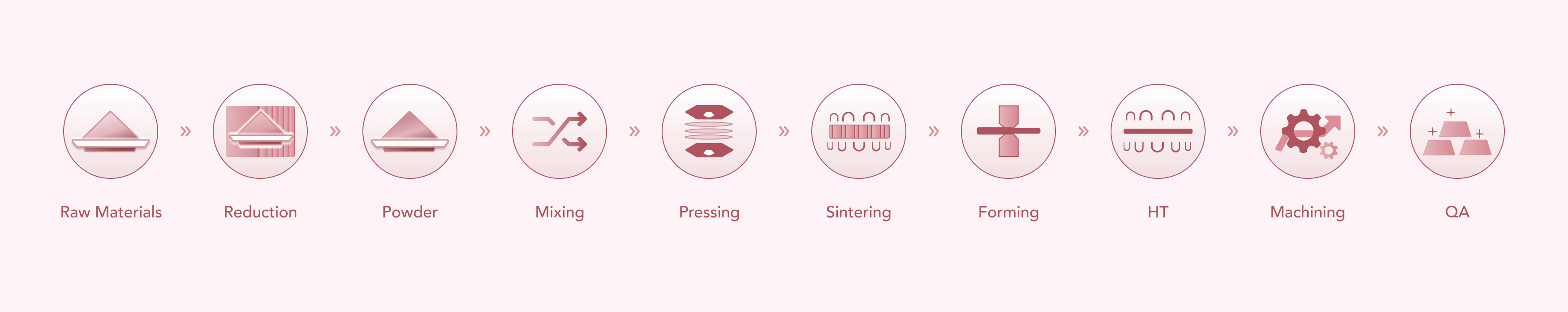
The Tin Selenide (SnSe) Target stands out due to its unique blend of structural integrity, electrical efficiency, and thermal characteristics, making it indispensable in thin film deposition processes. SnSe crystallizes in an orthorhombic layered structure, which facilitates anisotropic charge transport and exemplary thermoelectric performance. Manufactured with a high purity level of ≥99.9%, the SnSe target minimizes contamination during sputtering, ensuring high-quality thin films. With a melting point of approximately 861 °C and a density around 6.18 g/cm³, SnSe allows for uniform film deposition. Its semiconducting nature, featuring a narrow and adjustable bandgap (~0.9-1.3 eV depending on crystallographic orientation), provides precise control over the electronic and optical properties of the deposited films. Additionally, SnSe boasts low thermal conductivity and a high Seebeck coefficient, making it ideal for efficient energy harvesting applications. The target’s mechanical robustness and chemical compatibility with a variety of substrates further enhance its suitability for high-efficiency thermoelectric, optoelectronic, and photovoltaic devices.
Related Products: Tin Sputtering Target, Sn, Tin Zinc Sputtering Target, Sn/Zn, Selenium Sputtering Target, Se, Bismuth Selenide Sputtering Target, Bi2Se3
Material: Tin Selenide (SnSe)
Purity: 99.9%
Melting Point: 861 °C
Density: 6.18 g/cm³
Shape: Planar Disc
Sputtering Methods: RF, RF-R, DC
Bonding Types: Indium, Elastomer
Note: Specifications are based on theoretical data. For customized requirements and detailed inquiries, please contact us.
Custom sizes are available to meet specific project needs.
The Tin Selenide (SnSe) Target is extensively utilized in the production of thin films for a variety of cutting-edge applications, leveraging its exceptional thermal, electrical, and structural properties:
Our SnSe Targets are carefully packaged to ensure their protection during shipping and storage. Depending on the size, smaller targets are securely placed in polypropylene (PP) boxes, while larger targets are shipped in custom wooden crates. We prioritize customized packaging solutions and use appropriate cushioning materials to guarantee maximum protection.
Packaging Options:
Q1: What is the purity level of SnSe targets provided by SAM?
A1: SAM offers SnSe targets with a purity of 99.9% or higher, ensuring high-performance thin film deposition and minimal contamination.
Q2: What sputtering methods are compatible with SnSe targets?
A2: SnSe targets are compatible with RF and DC magnetron sputtering, depending on the specific equipment and film requirements.
Q3: How should Tin Selenide targets be stored?
A3: SnSe targets should be stored in a dry, inert environment to prevent oxidation or degradation, as selenium compounds can be sensitive to moisture and air over time.
| Property | SnSe Target (Tin Selenide) | Bi₂Te₃ Target (Bismuth Telluride) | PbTe Target (Lead Telluride) |
|---|---|---|---|
| Purity | ≥99.9% (polycrystalline, post-treatment) | ≥99.5% (Te contamination) | ≥99.0% (Pb volatility) |
| Density (g/cm³) | 6.2-6.5 (95% theoretical) | 7.7-7.9 (~98%) | 8.2-8.5 (~97%) |
| Thermal Stability (°C) | 500-800 (polycrystalline, oxide-free) | ≤450 (Te sublimation) | ≤700 (oxidation) |
| Thermal Conductivity | 0.07-0.32 W/m·K | 1.5 W/m·K | 2.0 W/m·K |
| Mechanical Strength | Flexural strength: 250-300 MPa | 50-100 MPa (brittle) | 80-120 MPa (cracking risk) |
| Sputtering Rate | 120-180 nm/min (DC, 500W) | 80-100 nm/min (RF, 300W) | 90-130 nm/min (DC, 400W) |
Physical Properties:
Chemical Properties:
Tin is a soft, malleable, silvery-white metal with atomic number 50, belonging to Group 14 of the periodic table. It has a relatively low melting point of approximately 231.9 °C and a density of 7.31 g/cm³. Renowned for its excellent corrosion resistance, tin forms a protective oxide layer that prevents further oxidation, making it ideal for coating other metals to prevent rusting (e.g., tin-plated steel). Tin is also a crucial component in various alloys, such as bronze (with copper) and solder (with lead or silver). Its good electrical conductivity and chemical stability support its use in electronics, coatings, and advanced materials.
Industrial Applications:
Physical Properties:
Chemical Properties:
Selenium is a non-metallic element with atomic number 34, known for its semiconducting and photoconductive properties. It readily forms stable compounds with metals, playing a crucial role in controlling bandgap energies and chemical reactivity during sputtering processes. Selenium is essential in thin film electronics and photovoltaic materials, contributing to the efficiency and performance of solar cells.
Industrial Applications: